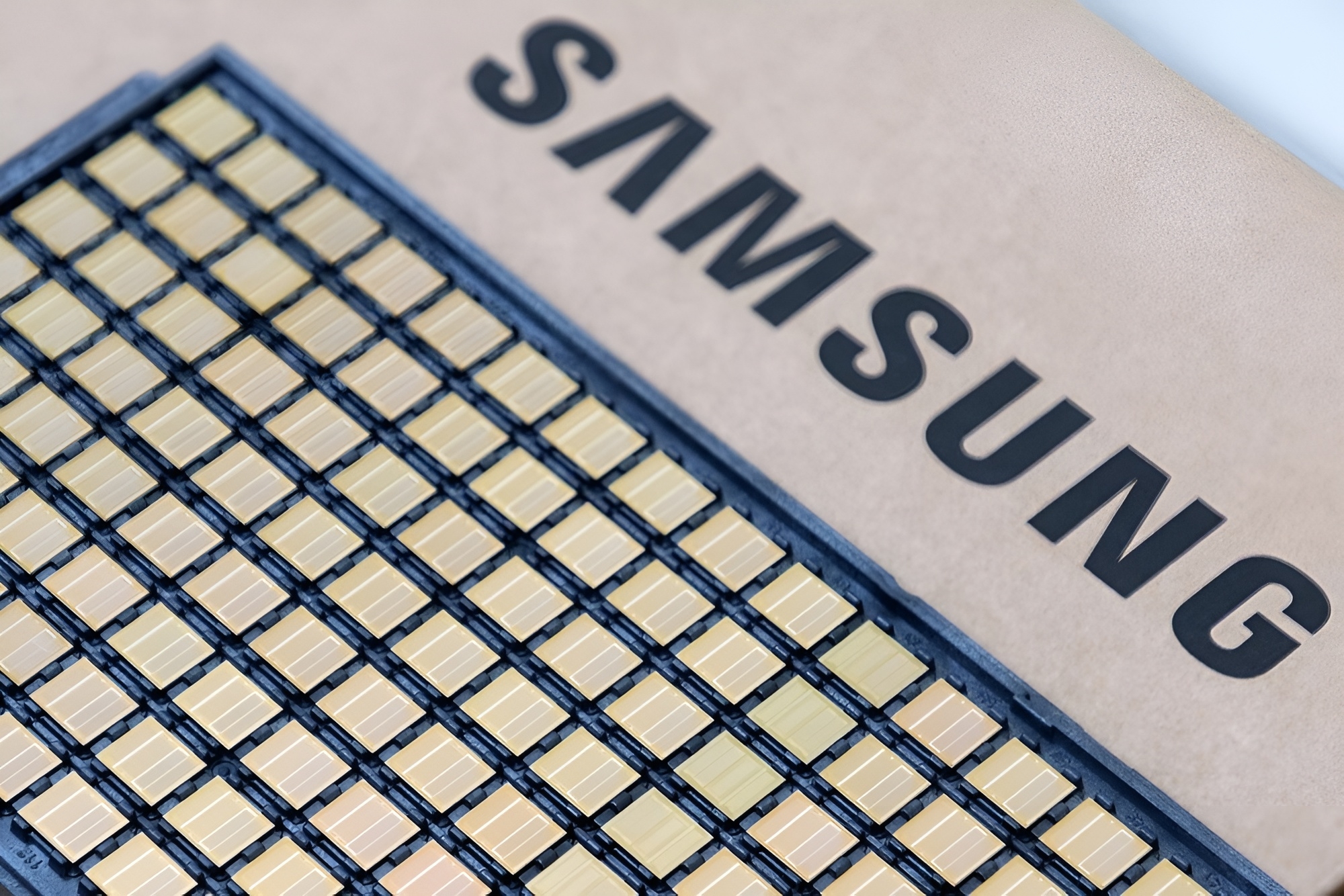
Samsung has suffered a major setback in its pursuit of high-end memory.Since the yield rate of key basic technology D1d DRAM failed to meet internal targets, Samsung has decided to indefinitely postpone the mass production plan of the next generation HBM5E memory.The D1d DRAM in question this time is Samsung’s seventh-generation 10-nanometer process, which was originally the core foundation of future HBM solutions. According to the plan, this technology will be used in the ninth-generation HBM product HBM5E.
Although the technology had previously received pre-production approval, yields continued to fall below target levels, making the return on investment for trial operations, let alone mass production, questionable.
According to people familiar with Samsung's internal situation, Samsung plans to restart mass production until the D1d yield rate reaches the target level. The current recovery timetable is not determined at all. Samsung is internally reviewing the process roadmap in an attempt to further improve the yield rate.
It is worth noting that Samsung’s existing 1c DRAM technology is currently being stably used in three generations of HBM products, including HBM4, HBM4E and HBM5.
HBM4 is expected to launch later this year. Nvidia's Vera Rubin and AMD's MI400 platforms will use HBM4, and HBM4E is expected to be used in Rubin Ultra and MI500 accelerators.
In the future, HBM5 and customized designs are expected to be adopted by NVIDIA's Feynman series and other solutions.
Samsung was previously reported to be significantly shortening the HBM development cycle and preparing new solutions at an unprecedented speed. However, fast development does not mean that mass production can be directly carried out. The production cycle has now become the biggest bottleneck.
At the same time, Samsung is also increasing its production capacity. It has invested additional resources in building a large-scale chip factory in Onyang, South Korea, with an area equivalent to four football fields. It is specially used to produce next-generation DRAM products including HBM. The factory will be responsible for key aspects such as packaging, testing, logistics and quality control.
Samsung's old rival SK Hynix has completed research and development on D1d DRAM technology and ensured yield.
Both parties are currently competing for large orders from leading AI companies. Whoever can make HBM planning more flexible and achieve continuous R&D and production while ensuring yield and stable return on investment will have the last laugh.