Recently, a source revealed thatThe yield rate of Samsung's DRAM chips based on the 1dnm process (seventh-generation 10nm-level process) during the trial production phase was lower than expected. Samsung has planned to postpone large-scale mass production indefinitely until the yield rate reaches the established target.To this end, Samsung may comprehensively review the process flow to further improve the yield rate.
According to the original plan,Samsung plans to use DRAM chips manufactured in the 1dnm process for HBM5E, the ninth-generation HBM solution.
It is worth noting that in addition to HBM4, DRAM chips currently using the 1cnm process will also be used in HBM4E and HBM5, covering three consecutive generations of HBM products. There are also rumors that Samsung may upgrade the basic die of the next generation HBM and switch to a more advanced 2nm process.
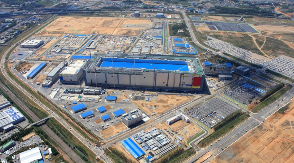
Currently, Samsung has invested more resources in 1dnm process DRAM chips and built a new factory in South Korea.
It is reported that,The factory covers an area about the size of four standard football fields. In addition to producing DRAM chips, it will also undertake packaging, testing, logistics and quality control. These processes are crucial to maintaining stable production.