IBM recently announced the launch of the world's first sub-1 nanometer (sub-1 nm) chip technology, with the core being a new transistor architecture of 0.7 nanometers, or 7 angstrom nodes. The company said that this achievement marks that the semiconductor industry is still expected to continue to improve performance and energy efficiency as it approaches the physical limits of traditional manufacturing processes.
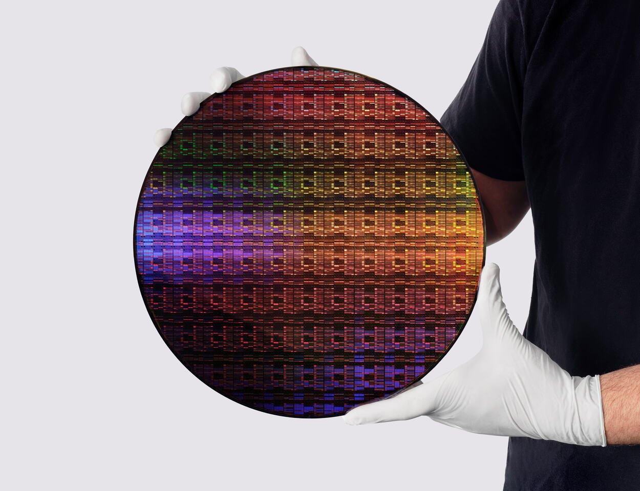
According to IBM, this chip can integrate nearly 100 billion transistors on a chip the size of a fingernail, almost twice as dense as the 2-nanometer chip it will release in 2021. Related technologies rely on a series of structural and material innovations, especially the three-dimensional "Nanostack" architecture proposed by IBM, which aims to advance chip manufacturing to an era close to the atomic scale.
IBM said that public technical results show that this new process can bring up to 50% performance improvement or 70% energy efficiency improvement compared to 2nm node chips, and is suitable for scenarios such as generative AI, cloud infrastructure, and next-generation electronic equipment. Jay Gambetta, head of research at IBM, said that this breakthrough means that chip technology is moving from the nanometer era to the atomic scale and will lay the foundation for the next stage of computing power.
"Nanostack" is described by IBM as the industry's first known three-dimensional, nanosheet-based transistor design. This architecture uses 3D sequential integration to increase the number of transistors per unit chip by stacking transistors vertically and staggering them. It can also use different material combinations in different stacked layers to optimize the performance and power consumption of each layer of transistors.

IBM also stated that this architecture has proven its practical manufacturing and computational feasibility through CMOS integration of ultra-thin dielectric bonding, demonstration of dual-channel engineering capabilities, and functional verification of CMOS inverters with expected switching performance. At the same time, new research presented by IBM at VLSI 2026 shows that the Nanostack architecture can enable SRAM to achieve a 40% scaling improvement, helping to meet the high-bandwidth data requirements of advanced AI workloads.
IBM pointed out that as logic technology breaks below the 1-nanometer node for the first time, the chip manufacturing process is entering the "angstrom-level" scaling stage. The company believes that although node names now represent more manufacturing generations than precise physical dimensions, its 0.7nm technology still proves that continued scaling is feasible and provides a roadmap for process evolution for at least the next decade.

In terms of industrial layout, IBM stated that this research and development was completed at the semiconductor research facility in Albany, New York, which will be equipped with High NA EUV lithography equipment in the future. IBM is also collaborating with partners such as Lam Research, Tokyo Electronics and SCREEN Semiconductor Solutions to develop High NA EUV processes and tools, and said that relevant work has produced working devices.
IBM also mentioned that the company also recently announced that it will establish Anderon, the world's first pure quantum foundry. According to IBM, as Nanostack technology is expected to enter sub-1 nanometer node applications as early as the next five years, the relevant mass production path is expected to appear as early as the next five years or so.