Intel's foundry business recently held a groundbreaking ceremony in Santa Clara, California, USA, officially launching the construction of a new local advanced manufacturing facility to further expand production capacity and technology layout in the core area of Silicon Valley.
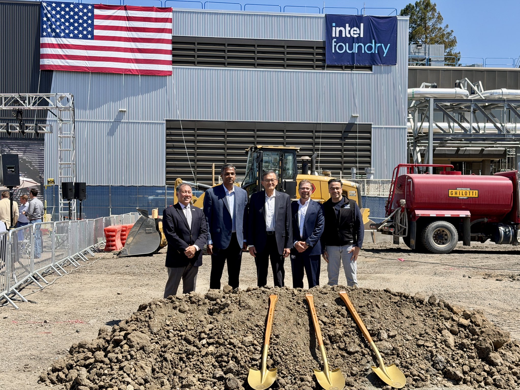
According to on-site information, Intel CEO Lip-Bu Tan and a number of senior executives attended the groundbreaking event to break ground for Intel’s new expansion project at the Bowers campus in Santa Clara. Intel executives attending the ceremony included James Chew, Naga Chandrasekaran, who is responsible for federal business, Frank Abboud, vice president of Intel's foundry business and general manager of mask operations, and Pushkar Ranade, Intel's chief technology officer.
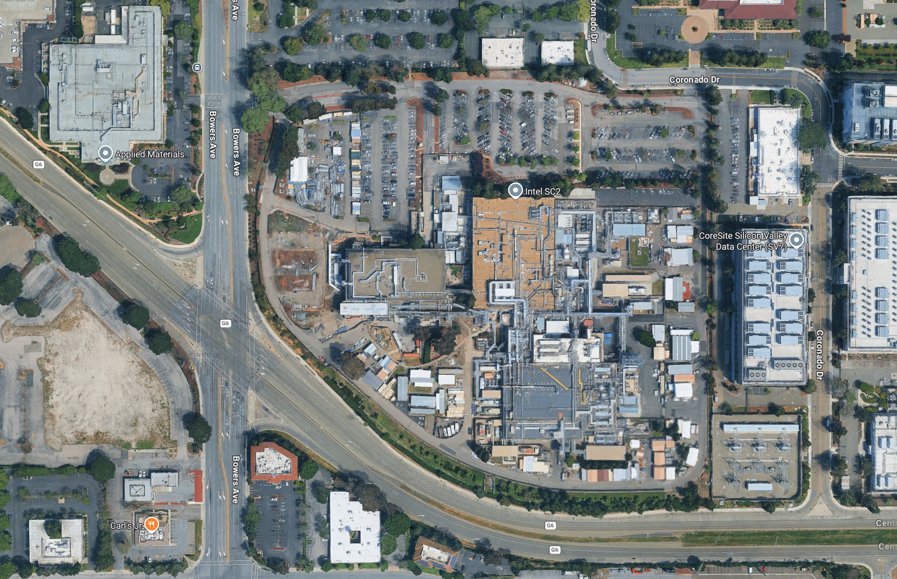
Intel has previously announced plans to add approximately 107,000 square feet of floor space at its Bowers campus in Santa Clara. This expansion will build two new three-story buildings for chip manufacturing, process processing and key public engineering facilities, providing greater production capacity and more complete infrastructure for Intel's foundry business.
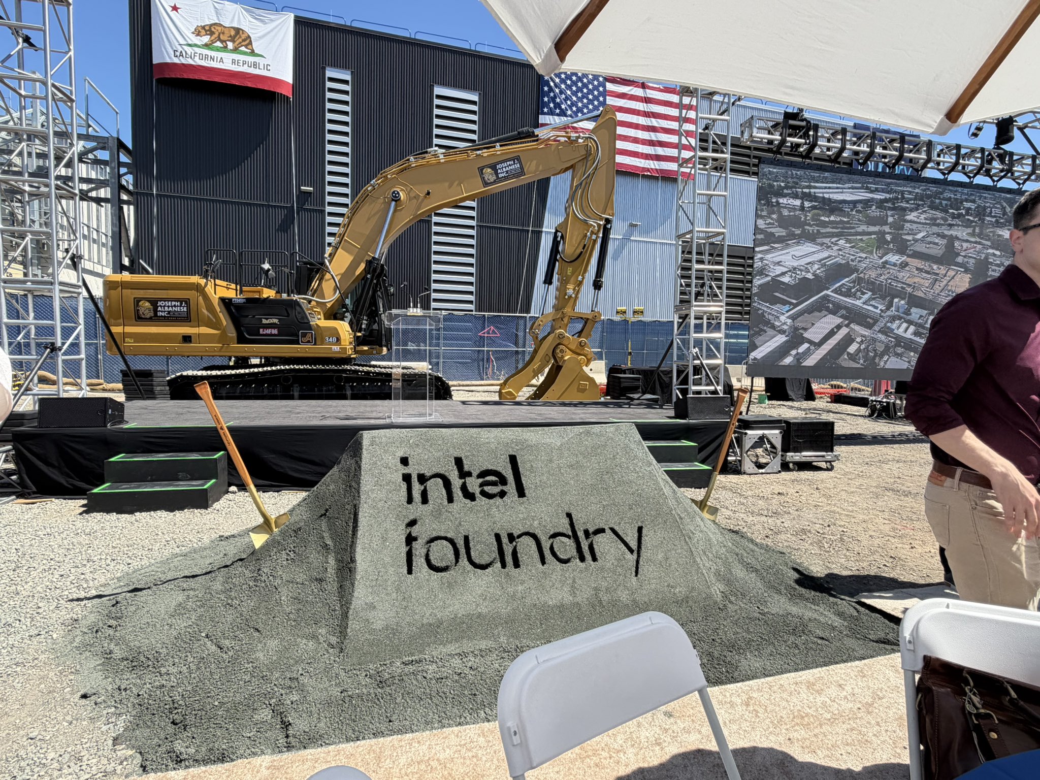
Construction on the new facility is expected to begin in mid-2026, and the current groundbreaking is well aligned with that timeline. Intel said this investment will further strengthen the company's "Made in the US" strategy and reflect its long-term commitment to the local Santa Clara and greater Silicon Valley semiconductor manufacturing ecosystem.
From the perspective of functional positioning, the expansion of the Bowers campus will become a key link in Intel's advanced process route, especially playing an important role in the production of masks (reticle) required for extreme ultraviolet (EUV) lithography. EUV masks are an indispensable basic link in realizing future advanced processes and will directly support Intel's mass production preparations for next-generation process nodes such as 18A-P and 14A.
Intel has repeatedly emphasized that process nodes such as 18A-P and 14A, as well as innovative solutions such as its advanced packaging technology and glass core substrates, will constitute the core competitiveness of Intel's foundry business for many years to come. As these technologies gain more trust and attention among external customers, the foundry business is seen as an important step for Intel to regain its global semiconductor leadership.
Industry insiders pointed out that Intel's foundry business is currently developing strongly, and the company continues to invest in future process nodes, advanced packaging and material innovation, which has aroused the interest of many large customers. The continued increase in manufacturing investment in the United States will, on the one hand, help increase customers' confidence in the security and controllability of the supply chain, and on the other hand, it also echoes the policy direction of the U.S. government to enhance local chip production capabilities.
Intel said that with the completion of the new facility in Santa Clara, the Bowers campus' capabilities in mask production, manufacturing support and related supporting services will be significantly enhanced, providing stronger support for future processes including 18A-P and 14A. This timely investment not only solidifies customers' trust in Intel's advanced technology, but also further demonstrates the company's firm commitment to "Made in America" and the long-term prosperity of the Silicon Valley semiconductor ecosystem.