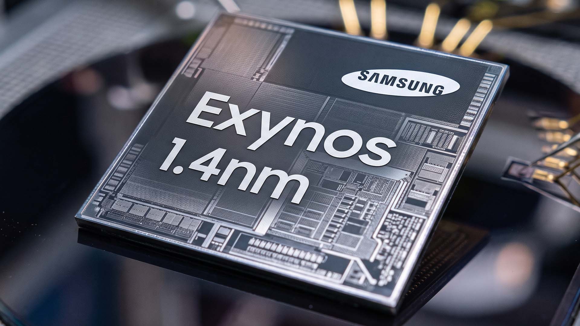
Samsung’s competitive strategy in the cutting-edge foundry field is quietly changing. The latest exposure of the Exynos series processor roadmap shows that the South Korean technology giant is not eager to advance in the process, but plans to work on its 2nm Gate All Around (GAA) process node for several years, which means that the launch of its first 1.4nm Exynos chip may require three generations of product changes.
Although this strategic adjustment may allow TSMC to seize the opportunity in the more advanced 1.4nm process, industry analysts believe that for Samsung, which has long been troubled by yield problems, this move can be regarded as a long-term good medicine.
According to the details disclosed so far, TSMC is expected to start mass production of its 1.4nm process as soon as 2028. In contrast, Samsung's pace of commercializing its 1.4nm node will be delayed until around 2029, nearly a year behind its competitors. Specific to the product line, Samsung's first chip to enter the 2-nanometer field will be the Exynos 2600, and the subsequent Exynos 2700 and Exynos 2800 are expected to continue to stick to the 2-nanometer camp. Among them, Exynos 2800 may use the third-generation 2-nanometer GAA process called SF2P+ to optimize the performance, power consumption and area performance of the chip through gradual iterations. It will not be until the replacement of these three generations of products is completed that the Exynos 2900, the first 1.4nm SoC, will officially debut.

In the past, Samsung was often keen on launching a fierce "first launch" battle with TSMC on process technology in order to win the attention of the industry in a short period of time. However, facts have proven that if yield cannot be guaranteed, radical process upgrades can easily bring heavy economic burdens to enterprises. Since TSMC's estimated cost of each 1.4nm wafer may be as high as US$45,000, Samsung's design unit (LSI) responsible for the Exynos brand is also facing similar huge quotations when purchasing wafers from its own foundry unit. If the process is not fully mature and the yield rate is low, the production cost of each Exynos chip will soar significantly.
Therefore, Samsung chose not to rush to launch the 1.4nm project, but instead focused on stabilizing and optimizing the 2nm process yield. By giving the 1.4nm process a more sufficient R&D and maturity cycle, it will not only ensure the commercial viability of the LSI department's subsequent products, but will also help Samsung's foundry business turn a profit as soon as possible. This shows that Samsung is seeking a more robust balance with a more pragmatic business attitude between pursuing leadership in surface technology and maintaining long-term corporate profitability.