According to reports from Reuters and other media, Chinese state-owned enterprise Shanghai Aishina Electronic Technology Group, in conjunction with Shanghai Microelectronics Equipment (SMEE) and Shanghai Electric Group and other institutions, has achieved the latest technological breakthrough in the field of domestic deep ultraviolet (DUV) chip manufacturing equipment. Although this development has attracted widespread attention at the social level, industry analysis reports point out that domestic DUV immersion lithography machines are still difficult to pose a direct threat to the existing market position of global industry giant ASML (ASML) in the short term.
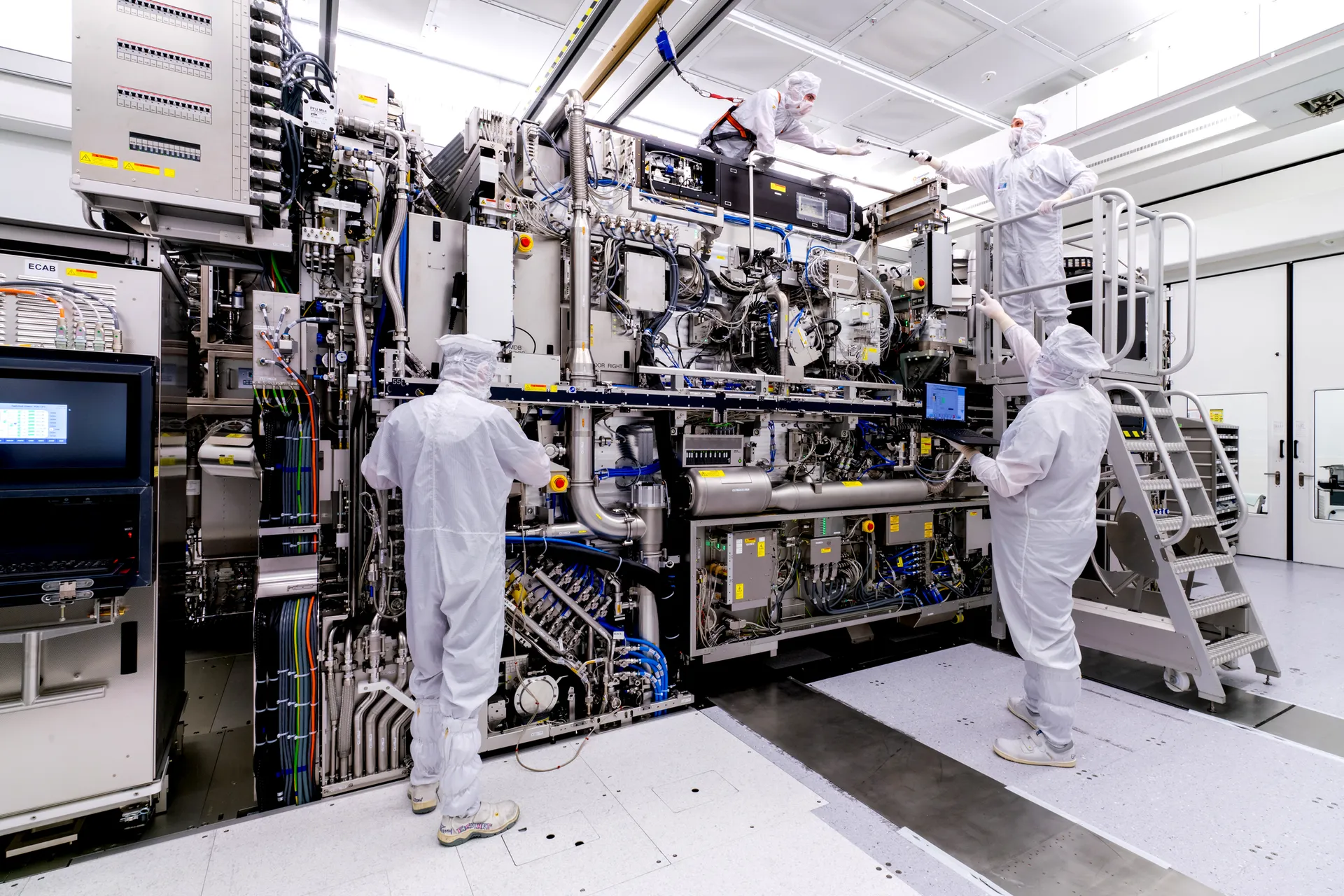
At present, export restrictions from Western countries mainly focus on advanced extreme ultraviolet (EUV) lithography systems, while there is no comprehensive embargo on DUV equipment with longer wavelengths and more mature processes. In the global market, Dutch manufacturer ASML's market control in the field of advanced DUV lithography machines is almost equal to its absolute monopoly in the field of EUV. Compared with EUV equipment, which requires a precise vacuum environment and extremely high technical barriers, DUV equipment mainly relies on a combination of laser and lens to print circuit patterns. It is still an indispensable basic equipment for China and even the global chip manufacturing industry.
Data shows that China is still one of ASML’s largest overseas markets. ASML's financial data for the first half of 2026 shows that the Chinese mainland market contributed approximately 2.6 billion euros in revenue, accounting for 16%, second only to Taiwan and South Korea. This also shows that China's semiconductor industry chain still maintains a high degree of dependence on ASML's technical equipment in the short term.
Industry expert analysis points out that domestic DUV lithography equipment still needs to go through a long and rigorous testing and verification phase before it can truly enter large-scale commercial applications. In addition, although the industry can use DUV equipment to produce chips close to or reaching the 7-nanometer process node through "Multi-patterning" technology, this method will significantly increase the defect rate and reduce the yield rate, thus driving up the production cost of a single wafer and limiting production capacity output.
Although there are reports in the industry that China has targeted the domestic mass production of EUV lithography machines around 2030, and technology giants such as Huawei are also accelerating the research and development of related core technologies, in terms of commercial yield and cost-effectiveness, the global supply chain barriers led by ASML will still be difficult to easily break in the short term.