
Abstract:
Chinese memory chip manufacturer Changxin Memory (CXMT) recently announced the progress of next-generation DRAM memory technology and plans to launch server DDR5 registered memory modules (RDIMM) using 4F² memory unit architecture by the end of 2026. Since Samsung Electronics was previously thought to not advance similar technology until around 2028, this timetable was once interpreted as indicating that Changxin Memory is expected to lead its Korean competitors in specific DRAM architectures by about two years.
Wall Street analysts, however, are cautious about the claim. Investment institution Rosenblatt believes that it is obviously too early to regard Changxin Storage’s technology roadmap as having achieved a decisive lead at this stage. Bank of America also pointed out that the United States’ export restrictions on advanced semiconductor manufacturing equipment may prompt Changxin Memory to rely more on innovation in memory unit structures rather than simply relying on more advanced photolithography processes to reduce chip area.
The core of this debate is not whether Changxin Storage has made technological progress, but whether its announced technical roadmap can truly be transformed into stable, low-cost, and large-scale commercial products that can be delivered. For the DRAM industry, releasing products, completing engineering verification, passing customer certification and achieving mass production are completely different stages.
According to Wccftech, Changxin Memory President Cao Kai recently introduced the company's 4F² DRAM technology progress at the Integrated Chip and Chiplet Conference held in Shanghai, and stated that it plans to launch server DDR5 RDIMM products based on this architecture before the end of 2026. If this plan is realized as scheduled, Changxin Storage will have the opportunity to introduce new storage unit architecture into the server memory market earlier.
However, as of now, Changxin Storage has not announced the complete performance specifications, final operating frequency, specific capacity, mass production yield and customer certification status of this product. Therefore, at this stage, it is not possible to judge whether it can fully compete with products from Samsung, SK Hynix and Micron in terms of performance, cost and reliability based on the release time alone.
4F² is a cell layout technology designed to increase DRAM storage density. To understand this technology, you need to first understand the basic structure of traditional DRAM memory cells.
Modern DRAM usually adopts a 1T1C architecture, that is, each memory cell consists of a transistor and a capacitor. The transistor is responsible for controlling the reading and writing of data, and the capacitor represents the data by storing electric charge. A large number of memory cells are arranged in an array composed of word lines and bit lines, forming the core storage area of the memory chip.
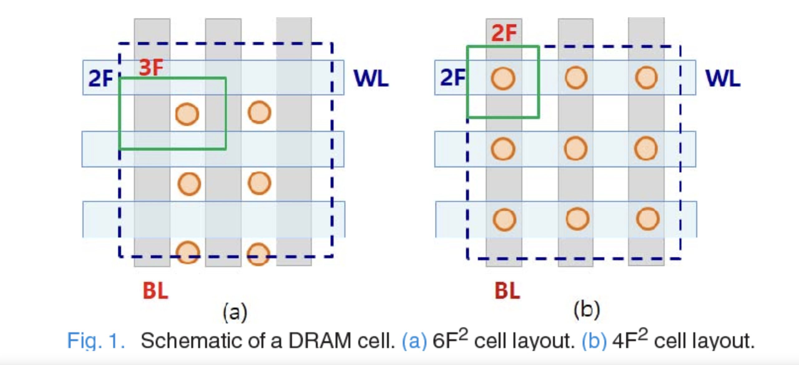
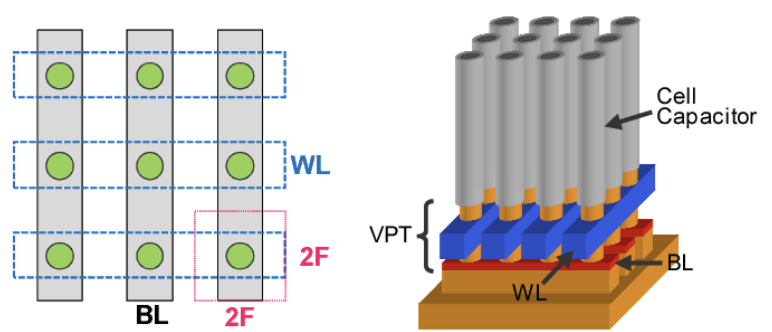
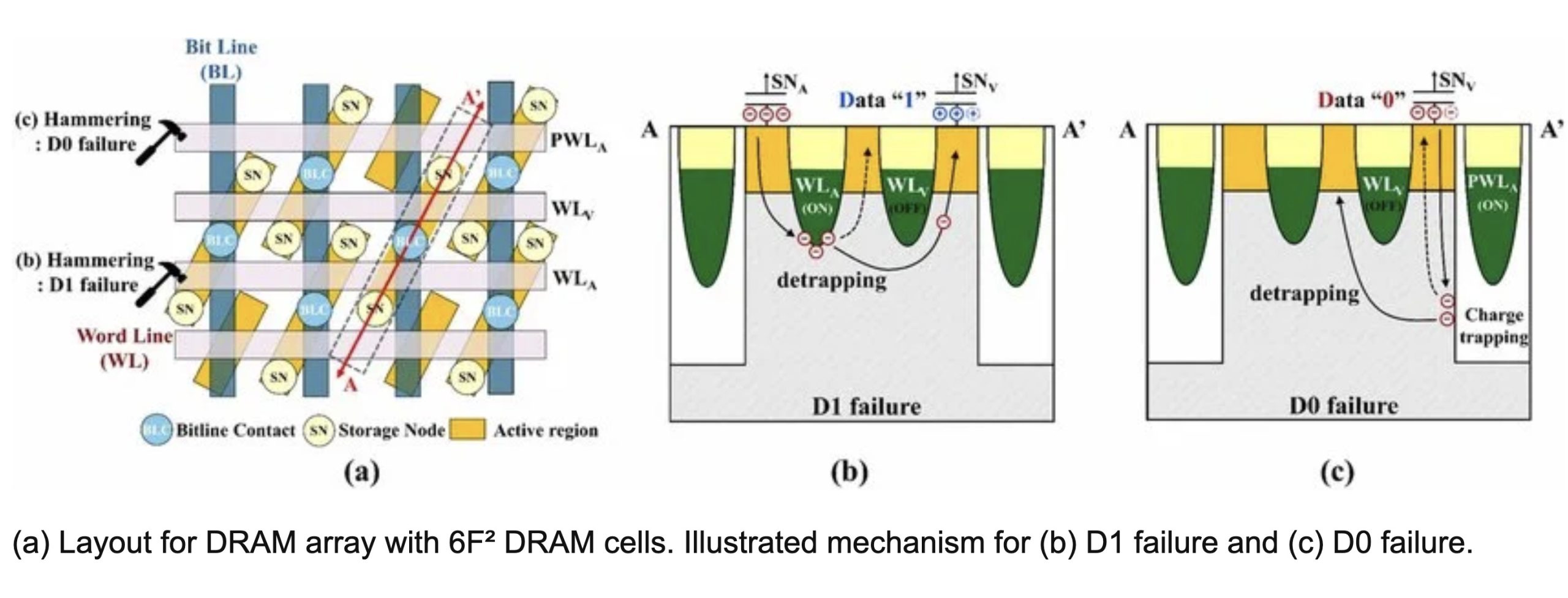
In the traditional 6F² layout, the theoretical floor area of a memory unit is 6F², where F represents the minimum feature size in process design. The 4F² layout attempts to compress the unit area to 4F² by changing the arrangement of the transistors and interconnect structures so that the transistors are arranged in the vertical direction instead of completely unfolding on the plane.
Under the same feature size, the theoretical area of 4F² memory cells is reduced by about one-third compared to 6F². This means that if peripheral circuits, other structures and manufacturing conditions permit, the chip can accommodate more memory cells in the same area, or reduce the chip area with the same storage capacity.
But there is a premise that is easily overlooked:
Reducing the unit area by one-third does not mean that the cost of the entire DRAM chip will also drop by one-third, nor does it mean that the performance will inevitably improve.
The storage array is only a part of the chip, and peripheral circuits, read and write circuits, redundant units and other structures also occupy the area. Final cost and density gains also depend on process integration, manufacturing yield and product design.The solution adopted by Changxin Memory is called a Vertical Surrounded Gate (VSG) transistor. Its transistor channels are arranged in a vertical direction, and the gate controls the channel from the surroundings, which helps to improve gate control and reduce leakage. With this structure, manufacturers have the opportunity to further reduce the area of a single storage unit.
Changxin Storage has not just started researching this direction recently. According to public reports, the company has conducted research on the 4F² architecture for many years and published relevant technical papers and patents. In 2023, the company also demonstrated the research results of a complete 8Gb storage array using this architecture. The company stated that it has accumulated more than 300 patent families around 4F² technology.
These research results show that 4F² is not just in the conceptual design stage. But there is still a considerable gap between research samples, full array demonstrations and mature commercial DRAM products. The real challenge is how to achieve stable electrical characteristics in a high-density structure and ensure that the chip has a high enough yield for mass production.
Bank of America: Export restrictions may prompt Changxin Storage to shift to 4F² structural innovation
Bank of America analysts believe that Changxin Memory’s promotion of 4F² technology is related to the restrictions faced by China in acquiring advanced semiconductor manufacturing equipment. After advanced lithography equipment is subject to export controls, it is difficult for Chinese memory chip companies to rely solely on continuously shrinking process sizes to increase storage density like Samsung, SK Hynix and Micron. Therefore, they are more motivated to find breakthroughs by changing the structure of memory cells.
In DRAM manufacturing, process shrinkage and memory cell structure innovation are two interrelated but not identical technical paths.
Process scaling mainly increases the number of memory cells that can be accommodated per unit area by reducing the size of key structures. 4F² attempts to change the layout of transistors in the memory array to reduce the theoretical area of the cell under the same feature size. The two can be used in combination and are not an either/or relationship.
There is still a gap between Changxin Memory’s current manufacturing capabilities and those of leading international manufacturers. Relevant reports pointed out that its 4F² products are expected to be built on the existing approximately 15-nanometer DRAM process platform, while manufacturers such as Samsung have advanced to the more advanced 10-nanometer DRAM process generation.
Therefore, even if Changxin Memory can be the first to bring 4F² products to the market, it does not mean that it is leading in all process indicators. It may make progress in memory cell structure, but it still needs to solve problems such as manufacturing accuracy, peripheral circuits, chip performance and overall cost.
However, Bank of America did not completely deny the potential competitiveness of this technology. If Changxin Memory can achieve large-scale production between 2027 and 2028, and Samsung, SK Hynix and Micron still have not commercialized similar architectures on a large scale, then Changxin Memory will have the opportunity to gain a competitive advantage in specific product areas.
This is also the reason why this technology release has attracted market attention. The DRAM industry has long been dominated by three manufacturers: Samsung, SK Hynix and Micron. Any new technology that may change the unit storage cost and increase chip density may affect the future competitive landscape of the three companies.
Rosenblatt: Technology roadmap cannot be directly equated with commercialization leadership
Compared with the relatively cautious attitude of Bank of America, Rosenblatt analysts are more skeptical about Changxin Storage's claim of technological leadership, believing that the so-called conclusion of leading competitors two years in advance currently lacks sufficient basis.
Rosenblatt pointed out that Samsung and SK Hynix are not not studying the 4F² architecture. Relevant companies have invested years of R&D resources, but this technology has not yet been widely used in commercial products. One reason is that while the 4F² structure increases density, it also brings new manufacturing problems.
As transistors, capacitors and related interconnect structures become more compact, process control may become more difficult. Small deviations in transistor size and location can affect the electrical performance of a memory cell. The tighter the structure, the more variables need to be controlled during the manufacturing process, and defects may be more difficult to avoid.
In addition, memory chips are extremely sensitive to yield. A DRAM chip contains a large number of memory cells. Even if the probability of a defect in a single cell is very low, it may accumulate into a significant yield loss in the entire array. Manufacturers must control defects through redundant design, testing and repair mechanisms to ensure that the final product meets commercial standards.
If the new architecture can increase the theoretical density, but leads to a decrease in yield, an increase in manufacturing costs, or insufficient product reliability, then it may not be more economical than the mature 6F² solution.
Rosenblatt’s doubt is based on this point: Changxin Memory’s announcement of plans to launch 4F² products does not mean that it has proven that it can achieve stable mass production at a competitive cost. To judge whether the technology is truly leading, you need to see actual products, reliable performance data, and commercial manufacturing results, rather than just comparing the timetables published by the two companies.
Samsung and SK Hynix are also promoting 4F² technology
From the perspective of industry development, 4F² is not a unique technical direction of Changxin Storage.
Samsung has previously publicly demonstrated a 4F² DRAM design using vertical channel transistors, and is studying wafer-level hybrid bonding technology to more flexibly integrate the memory cell array with peripheral circuits. Related technologies are expected to improve chip area utilization while increasing storage density.
Previous industry reports pointed to Samsung’s mass production time using the 4F² architecture as being around 2028. However, subsequent Korean media reports showed that the relevant technical routes and specific timetables are still subject to change, and 2028 cannot be regarded as the confirmed mass production date.
SK Hynix has also announced research plans surrounding vertical transistors, 4F² memory cells and three-dimensional DRAM. Micron’s related roadmap does not have a similarly clear public timetable.
Therefore, the so-called Changxin Storage is two years ahead is actually comparing Changxin Storage's target of launching products by the end of 2026 with the previously reported R&D or mass production time of its competitors. However, what different companies refer to as "launching products", "introducing technology" and "starting mass production" may respectively correspond to different stages such as engineering samples, customer samples, risk production or large-scale commercialization.
If we do not distinguish between these concepts and directly convert them into leading years, it is easy to exaggerate the technological gap.
The real test is whether it can stabilize mass production and gain recognition from server customers
The product Changxin Storage plans to launch this time is DDR5 RDIMM, which is a registered memory module for servers and workstations.
RDIMM usually uses a register or buffer mechanism to reduce the electrical load on the memory controller, allowing the server platform to support more memory modules and larger memory capacity. Compared with ordinary desktop memory, server memory has stricter requirements for reliability, stability, compatibility and long-term supply capabilities.
This also means that even if Changxin Memory successfully manufactures DRAM chips using the 4F² architecture, it must further complete module design, system compatibility testing and customer certification before it can enter the server market.
Data center customers will not immediately deploy a certain type of memory on a large scale just because it uses a newer storage unit structure. Memory must remain stable under different loads and meet requirements such as error control, temperature management, long-term operation and supply consistency. Problems in any link may affect the commercialization progress of the product.
As of the time of the release of relevant reports, Changxin Memory has not disclosed the complete capacity, operating frequency, chip density, final manufacturing process, mass production scale and customer list of the new product, and no third party has independently tested this 4F² product. Therefore, it is currently impossible to tell whether its actual performance is better than existing Samsung, SK Hynix or Micron products.
If the company can launch the product as planned and gradually prove its yield, stability and cost advantages, then this technology may become an important development for China's DRAM industry. On the contrary, if the product launch time is delayed, or if it faces yield and cost problems after mass production, then the so-called lead two years in advance will be difficult to establish.
From the perspective of industrial competition, Changxin Memory can no longer simply be regarded as a marginal player in the international DRAM market. Its fifth-generation G5 DRAM platform has entered mass production and its market share is also growing. TrendForce data shows that Changxin Memory’s share of global DRAM revenue reached 9.5% in the second quarter of 2026, higher than 7.6% in the first quarter, ranking fourth in the world.
This shows that Changxin Storage is gradually expanding its business scale and has the ability to invest more resources in the research and development of new architectures. However, growing market share and mastering next-generation storage technology are still two different things. Just because the former has made progress, it cannot be directly concluded that the latter has been successful.
Overall, Changxin Memory’s 4F² DDR5 plan is worthy of attention, but at this stage it is more suitable to regard it as a technology route with potential that still needs to be commercialized, rather than an established generational leadership.
The 4F² architecture can indeed increase the density of storage cells in theory, and Changxin Memory has also accumulated corresponding research and patent foundations. However, whether this technology can change the global DRAM market pattern ultimately depends on whether the product can be launched on schedule, whether the manufacturing yield can meet the requirements, whether the unit storage cost is competitive, and whether server customers are willing to adopt it on a large scale.
For Samsung, SK Hynix and Micron, the progress of Changxin Memory deserves continued attention; but for the entire industry, the truly decisive node is not to announce the adoption of a new architecture, but to transform it into a stable, reliable, and sustainably profitable mass-produced product.
Comments