
Abstract:
In the context of the explosion of global computing power demand driven by artificial intelligence, the semiconductor industry is experiencing a phenomenon that was almost unimaginable in the past: the market value per unit area of advanced DRAM wafers used to manufacture DDR5 memory has exceeded TSMC’s most advanced 2nm logic wafers.
The latest industry analysis shows that the current unit area value of 1b DRAM is approximately US$0.654 per square millimeter, while the corresponding unit area price of TSMC’s 2-nanometer (N2) wafer is approximately US$0.424 per square millimeter. In other words, for a silicon wafer of the same size, the current market value of advanced DRAM is about 54% higher than that of TSMC’s most cutting-edge process.
This result surprised many people in the industry, because in terms of manufacturing difficulty, the two are not at the same level at all.
TSMC’s 2nm process represents one of the most advanced logic chip manufacturing technologies in the world. It requires the use of the most complex EUV lithography equipment, advanced transistor structures and extremely stringent manufacturing processes. Its process complexity is much higher than the DRAM manufacturing technology used in DDR5 memory.
However, market pricing does not operate according to manufacturing difficulty.
According to industry data, the price of a 300mm TSMC 3nm wafer is about US$20,000, while the price of a 2nm wafer of the same size is close to US$30,000. After conversion, the unit area price of 3-nanometer wafers is approximately US$0.283 per square millimeter, and that of 2-nanometer wafers is approximately US$0.424 per square millimeter.
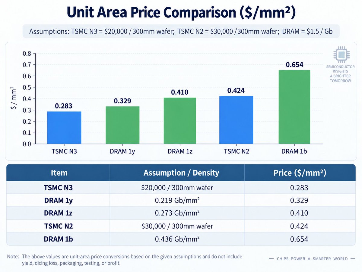
On the other hand, the current bit density of 1b DRAM reaches 0.436Gb per square millimeter. If calculated based on the market price of approximately US$1.50 per Gb, its corresponding value is approximately US$0.654 per square millimeter, surpassing TSMC's 2-nanometer wafer.
It is worth noting that this estimate is not a theoretical figure divorced from market reality.
Just recently, data released by market research organization DRAM Exchange shows that the price of 16Gb DDR5 eTT products is approximately US$24.80, corresponding to a price per Gb of approximately US$1.55. Therefore, the reference price of US$1.50 adopted by the analysis agency is considered to be highly reasonable.
What’s even more interesting is that even the technically obsolete 1z DRAM has a unit area value close to TSMC’s 2nm level.
Data shows that the bit density of 1z DRAM is about 0.273Gb per square millimeter. According to the same calculation method, its value is about $0.410 per square millimeter, almost the same as the $0.424 for 2nm wafers.
Industry analysts believe that this phenomenon does not mean that DRAM production costs have exceeded 2nm chips.
What has really changed is the relationship between market supply and demand.
Over the past many years, it has been generally believed that the most advanced logic processes represent the most valuable manufacturing resources in the semiconductor industry chain. However, as the demand for memory in artificial intelligence training servers, inference clusters, and high-performance computing platforms increases dramatically, DRAM has become one of the most scarce resources in the entire industry.
In particular, prices of DDR5, high-bandwidth memory and various advanced storage products for AI systems continue to rise amid continued market shortages, thus driving the value per unit area to continue to rise.
Analysts pointed out that the current high prices given by the market essentially reflect scarcity, not manufacturing difficulty.
Although manufacturers such as Samsung, SK Hynix and Micron continue to expand production, the AI industry's demand for memory is still growing faster than new supply. A large number of AI servers not only require advanced GPUs, but also require a large amount of DRAM, which has caused long-term tension in the entire storage industry.
Meanwhile, a more expensive new generation of DRAM technology is on the way.
For example, Samsung has adjusted its next-generation DRAM development route and advanced hybrid bonding technology ahead of schedule. Future high-end DRAM will adopt more complex manufacturing methods. The memory cells and peripheral control circuits will be manufactured separately and then integrated through wafer-level hybrid bonding.
Due to the significant increase in the cost of this new process, the industry predicts that the price of advanced DRAM products is likely to remain high in the future.
For the entire semiconductor industry, this phenomenon releases an important signal: In the era of artificial intelligence, the factor that determines value is no longer just the complexity of the manufacturing process, but what resources are truly scarce in the market. At the current stage, one of the most scarce resources in the world is no longer simply advanced logic processes, but large-capacity, high-performance memory that can support the operation of AI systems.
Comments