
Abstract:
As the demand for high-bandwidth memory in artificial intelligence data centers continues to grow, Samsung Electronics is accelerating the expansion of next-generation HBM production capacity. The latest news shows that Samsung plans to at least double the production of HBM4 series products in 2027, including the sixth-generation high-bandwidth memory HBM4 and the subsequent HBM4E.
At the same time, Samsung is also significantly increasing the processing capacity of glass substrates required in the HBM production process, which is seen by the industry as the company is preparing in advance for larger-scale high-stack HBM production.
According to semiconductor industry sources, Samsung plans to increase the outsourced glass substrate cleaning volume to about 50,000 pieces per month next year, while the average monthly volume this year is about 20,000 pieces, and only about 10,000 pieces in 2025. In other words, Samsung increased this production capacity demand to five times its original value in two years.
Glass carrier is a temporary support material used during HBM production. When DRAM wafers go through processes such as thinning and drilling, as the wafer becomes thinner and thinner, it is easy to bend or even break. Therefore, a glass carrier needs to be temporarily attached to the back of the wafer for support. As HBM develops from 8 and 12 layers to higher layers, single DRAM die needs to be further thinned, and the importance of wafer warpage control and related support processes has also increased.
Samsung is currently expanding production of HBM4 and HBM4E, which mainly use high-stack structures of 12 layers and above, so the usage of glass carriers can reflect the production scale of related products to a certain extent. Although the glass carrier plate can be reused after cleaning, and different production processes and yields will also affect actual consumption, industry insiders believe that the increase from 20,000 pieces per month to 50,000 pieces can still reflect Samsung's expansion trend of at least doubling the output of the HBM4 series.
Samsung has started mass production and shipped HBM4 to customers in February this year, using the sixth-generation 10-nanometer 1c DRAM process and the 4-nanometer logic base chip of Samsung's foundry department. The HBM4 product officially announced by Samsung has a stable transmission speed of 11.7Gbps, the maximum speed can reach 13Gbps, and the maximum bandwidth of a single stack reaches 3.3TB/s. Samsung also offers a 12-layer stacking version and plans to use 16-layer stacking technology to further expand capacity.
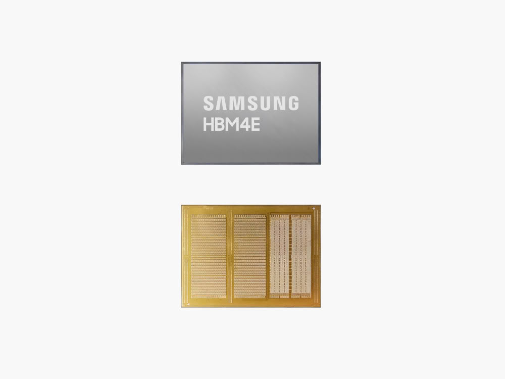
In terms of HBM4E, Samsung has begun to provide 12-layer samples to major customers including NVIDIA in May this year. Samsung's official data shows that its 12-layer HBM4E has a capacity of 48GB, a stable pin speed of 14Gbps, and can be further increased to 16Gbps, and a single stack bandwidth of up to 3.6TB/s. Compared with the previous generation product, HBM4E's energy efficiency is improved by approximately 16%, and its thermal resistance performance is improved by more than 14%.
Samsung has previously stated that HBM4E will use the same 1c DRAM core process and 4nm logic substrate technology as HBM4, thereby minimizing the time for product upgrades from HBM4 to HBM4E. The company plans to arrange mass production of HBM4E according to the customer's product schedule.
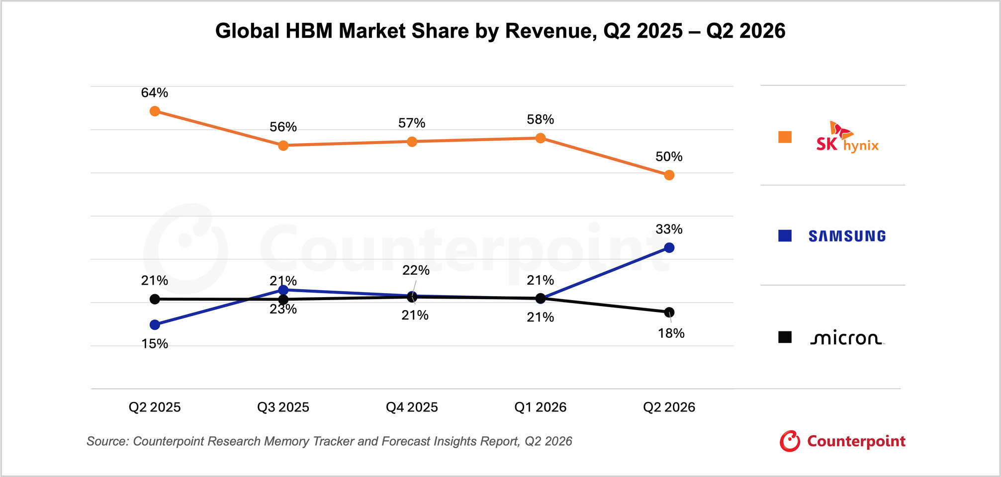
From the perspective of overall production capacity, the industry predicts that Samsung's monthly HBM wafer investment in 2027 may increase from approximately 180,000 wafers in 2026 to approximately 250,000 wafers, an increase of nearly 40%. However, compared with the growth of total production capacity, the change in product structure may be more obvious.
The HBM4 series is expected to account for about 80% of Samsung's overall HBM shipments from about 40% in 2026. This means that Samsung’s future HBM production expansion is not just about simply increasing the number of products, but is clearly tilting towards new-generation high-end products such as HBM4 and HBM4E.
This adjustment is closely related to the strong demand for HBM in the current AI infrastructure market. As companies such as NVIDIA launch new generations of AI accelerators, GPUs and AI-specific chips require increasingly larger memory bandwidth and capacity, and HBM has become a key component in high-performance AI computing systems. Since HBM's production requires multiple links such as DRAM manufacturing, wafer thinning, TSV, and advanced packaging, its capacity expansion speed is usually difficult to quickly keep up with the growth in AI server demand.
Samsung has previously revealed that its HBM production capacity in 2026 has basically been booked by customer orders, and the company expects full-year HBM sales to more than triple compared to 2025. At the same time, Samsung also stated that even if it continues to expand production, the current demand for HBM from major customers still exceeds the supply the company can provide, so some customers have begun to discuss 2027 and longer-term supply with Samsung in advance.
This is also one of the reasons why Samsung is expanding the production capacity of HBM3E, HBM4, and HBM4E at the same time. Companies need to prepare for orders for next-generation products while meeting current AI accelerator needs. Samsung has previously stated that it will continue to expand 1c DRAM production capacity and make early investments in HBM4 and HBM4E.
From a technical perspective, one of the core changes between HBM4 and HBM4E is the higher number of stacking layers and larger data I/O scale. HBM4 increases data I/O from 1024 to 2048 in HBM3E, which can significantly increase bandwidth, but also increases power consumption and heat dissipation pressure. Samsung reduces power consumption through low-voltage TSV technology and power distribution network optimization, and improves thermal management inside the package.
As the number of HBM stack layers continues to increase, the requirements for wafer thinning, warpage control and packaging accuracy during the production process are also getting higher and higher. Therefore, Samsung has significantly increased the cleaning volume of glass substrates, which is also considered by the industry to be expanding infrastructure in advance for higher-layer HBM production.
However, capacity expansion does not mean that all these products will be converted into actual shipments. In particular, the future mass production scale of HBM4E also depends on the product certification, testing and actual needs of major customers. For Samsung, there's still a gap between how much capacity it can build and how much product it can ultimately deliver to customers.
At present, Samsung has entered the mass production stage in the HBM4 field and has begun to provide HBM4E samples to major customers. As the AI server and accelerator market continues to expand in 2027, Samsung is expected to focus more and more production resources on high-value products such as HBM4 and HBM4E. According to current industry forecasts, Samsung's HBM4 series production will at least double in 2027, and its proportion in the entire HBM product portfolio may also increase significantly from about 40% to about 80%, which means that Samsung is accelerating the shift of HBM business focus to a new generation of high-bandwidth memory.
Comments