
Abstract:
As demand for high-bandwidth memory (HBM) continues to rise in the artificial intelligence market, NVIDIA is driving an unprecedented supply chain integration plan. According to the latest news, the customized high-bandwidth memory NVHBM developed by NVIDIA for the next generation AI accelerator will prompt long-term competition between Samsung Electronics and TSMC to cooperate to jointly create a base chip (Base Die) based on the 3-nanometer process.
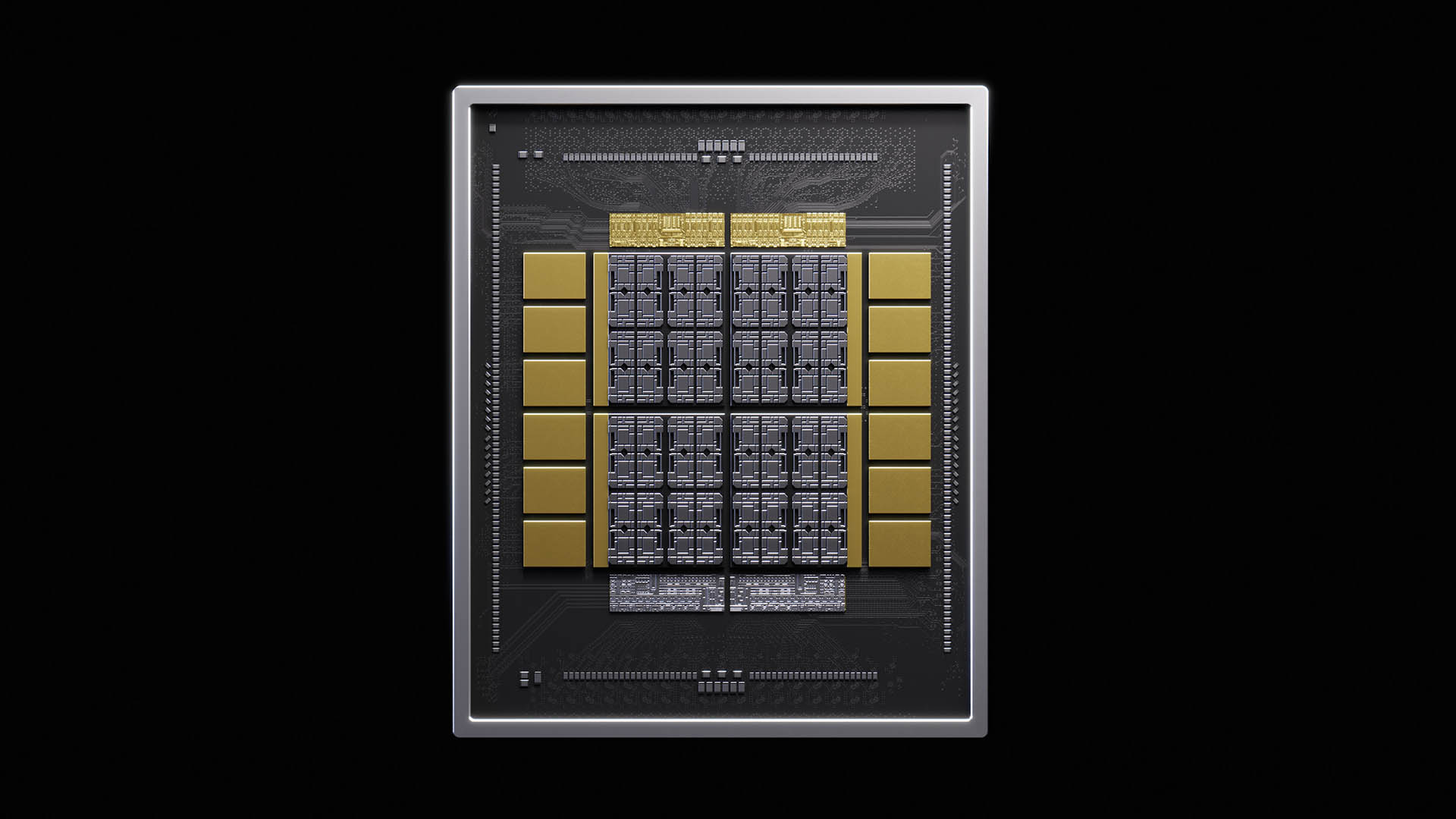
According to reports, Samsung has always adopted a "turnkey" model in HBM product development, that is, both the core memory chip (Core Die) and the base chip are designed and manufactured by itself. However, NVIDIA's customized version of NVHBM imposes stricter standardization requirements on the manufacturing process, so Samsung and TSMC are required to jointly participate in the development of 3-nanometer base chips to form unified product specifications and reduce subsequent quality verification steps.
In addition to Samsung, Micron and SK Hynix are also included in this plan. NVIDIA hopes that by unifying the manufacturing process, HBM products provided by different suppliers can achieve consistent performance. It has been previously reported that Feyman architecture GPUs will use customized HBM solutions in the future. NVIDIA said that compared to standard HBM4E products, NVHBM is expected to provide up to 30% additional memory bandwidth while reducing power consumption by up to 15%.
In order to achieve this goal, Nvidia requires Samsung, Micron and SK Hynix to uniformly use TSMC's 3nm process to produce NVHBM base chips. At the same time, the core memory chip needs to use the sixth-generation DRAM process, which is also called the "1c" process node.
The main reason for driving all suppliers to use the same manufacturing scheme is to ensure consistent performance of the final product. If all base chips are produced using TSMC's 3nm process, NVIDIA will not need to conduct independent verification for each supplier, thereby saving a lot of time and engineering resources and accelerating product introduction.
Samsung has reportedly accepted the request. This is also the first time that the company has abandoned the completely independent "turnkey" model for HBM products. However, Samsung has not completely given up its own foundry resources. The company is still evaluating its own foundry capacity plan to prevent future NVHBM demand from exceeding the production capacity that TSMC can provide.
At the same time, Samsung will still be responsible for the research and development of core chips and base chips for standard HBM products. Considering that the demand for HBM in the AI market continues to explode, even if it requires cooperation with its main competitor TSMC, Samsung is willing to accept this special arrangement to ensure that it can continue to participate in Nvidia's high-value AI supply chain.
For Samsung, HBM business is also becoming an important pillar in improving the financial performance of the foundry business. Previous industry data showed that the loss scale of Samsung's foundry department has shrunk from 6.74 trillion won in 2025 to 3.92 trillion won in 2026, a decrease of 41%. As the AI server and accelerator markets continue to expand, high-margin HBM products are seen as an important opportunity to help Samsung further improve profitability.
Analysts believe that Nvidia's promotion of NVHBM standardized production will not only help improve product performance consistency and supply efficiency, but also break the model of traditional storage manufacturers fighting each other. Against the background of increasingly fierce competition in AI infrastructure, Samsung and TSMC, which were originally in a fierce competition, formed a temporary partnership due to Nvidia's needs. This phenomenon highlights the increasingly profound impact of the artificial intelligence industry on the global semiconductor supply chain pattern.
Comments