
Abstract:
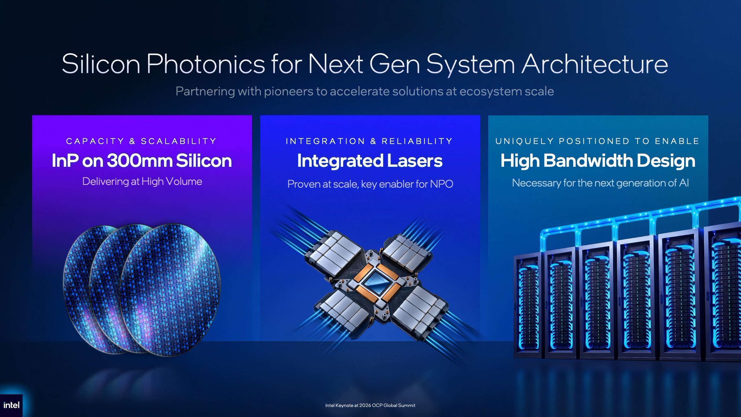
At the 2026 Open Compute Project (OCP 2026) Global Summit, Intel demonstrated the latest silicon photonics technology development blueprint, emphasizing that this technology will become an important foundation for future high-performance computing (HPC) and artificial intelligence (AI) data centers. Nic Dubé, vice president of Intel Data Center Systems and Solutions, described silicon photonics as the "Golden Hammer" of next-generation system architecture at the meeting, and pointed out that Intel is currently the only high-capacity foundry capable of large-scale mass production of 300 mm indium phosphide (InP) silicon photonics wafers.
As the scale of artificial intelligence accelerators continues to expand, how to quickly move data between massive graphics processing units (GPUs), central processing units (CPUs) and memory resources has become a key factor in determining overall system performance. Nick Dube said that traditional copper interconnects are increasingly approaching physical limits and are facing severe bottlenecks in terms of transmission distance, packaging edge bandwidth density, and transmission energy consumption per bit (pJ/bit). To break through these limitations, data center architecture must accelerate the evolution from traditional copper wires to optical interconnects and push energy consumption targets to less than 5 picojoules per bit (5 pJ/bit).

At the manufacturing and core technology levels, Nick Dube emphasized Intel's two core competitive barriers in the field of silicon photonics. First of all, Intel is currently the only wafer foundry in the industry with large-scale mass production capabilities for 300 mm indium phosphide silicon photonics, and has the ability to deliver this technology to the entire industry on a large scale. In the current optical transceiver market, the production capacity of laser chips and indium phosphide materials has been in short supply for a long time. Intel has directly integrated indium phosphide light source technology into the 300 mm large-size silicon wafer process, which has greatly improved manufacturing efficiency and production capacity. Second, Intel has a unique long-term proven track record in the reliability of integrated lasers. Since its commercial launch in 2016, Intel has been deeply involved in the field of silicon photonics for more than two decades and has shipped more than 8 million optical transceivers and 32 million integrated lasers. This proven reliability, proven in large-scale real-world deployments, is critical for system architectures looking to adopt integrated light source designs.
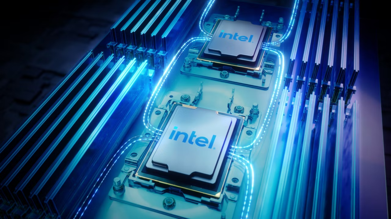
In terms of system-level applications and future evolution, Intel is relying on its 300mm silicon photonics process and integrated indium phosphide light source technology to fully promote the development of co-packaged optics (CPO) and near-packaged optics (NPO) technology to achieve higher density optical interconnections. By directly introducing optical interconnect interfaces at the packaging level, future AI and HPC infrastructure will not only solve the high-speed communication bottleneck between chips, but also extend optical interconnect from simple chip-level interconnect to larger-scale computing resource pooling and memory decoupling, thereby reshaping the overall system architecture of the next-generation artificial intelligence data center.
Comments