
Abstract:
During SEMICON Taiwan 2026 held in Taipei, Samsung announced its latest memory product roadmap, focusing on HBM5 and the new zHBM architecture. Samsung said that HBM5 aims to achieve approximately twice the overall performance compared to HBM4E, while increasing unit power consumption performance by 20% and reducing thermal resistance by 20%.

HBM5 will use Samsung’s self-developed 2nm process to manufacture the basic die, replacing the 4nm process used by HBM4 and HBM4E. The number of product stacking layers will also be expanded to 12, 16 and 20 layers, and it is expected to enter mass production around 2028.
Samsung also recently confirmed in the preview materials of the Hot Chips 2026 conference that the company is preparing to launch HBM4E, with a target speed of 16 Gbps per pin. The HBM4 currently being shipped by Samsung has a speed of 11.7 Gbps per pin.
Compared with the traditional HBM design that places the memory next to the accelerator, zHBM adopts a more radical vertical integration method, stacking the memory directly on top of the processor, thereby shortening the data transmission path and improving bandwidth and energy efficiency. Samsung predicts that zHBM’s raw performance will reach 8 times that of HBM4E, and its unit power consumption performance will reach 3 times, while reducing thermal resistance by 75% to 90%.
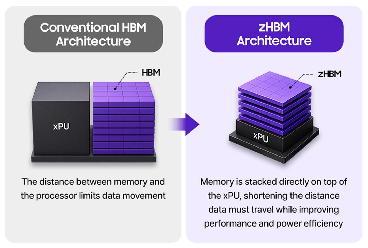
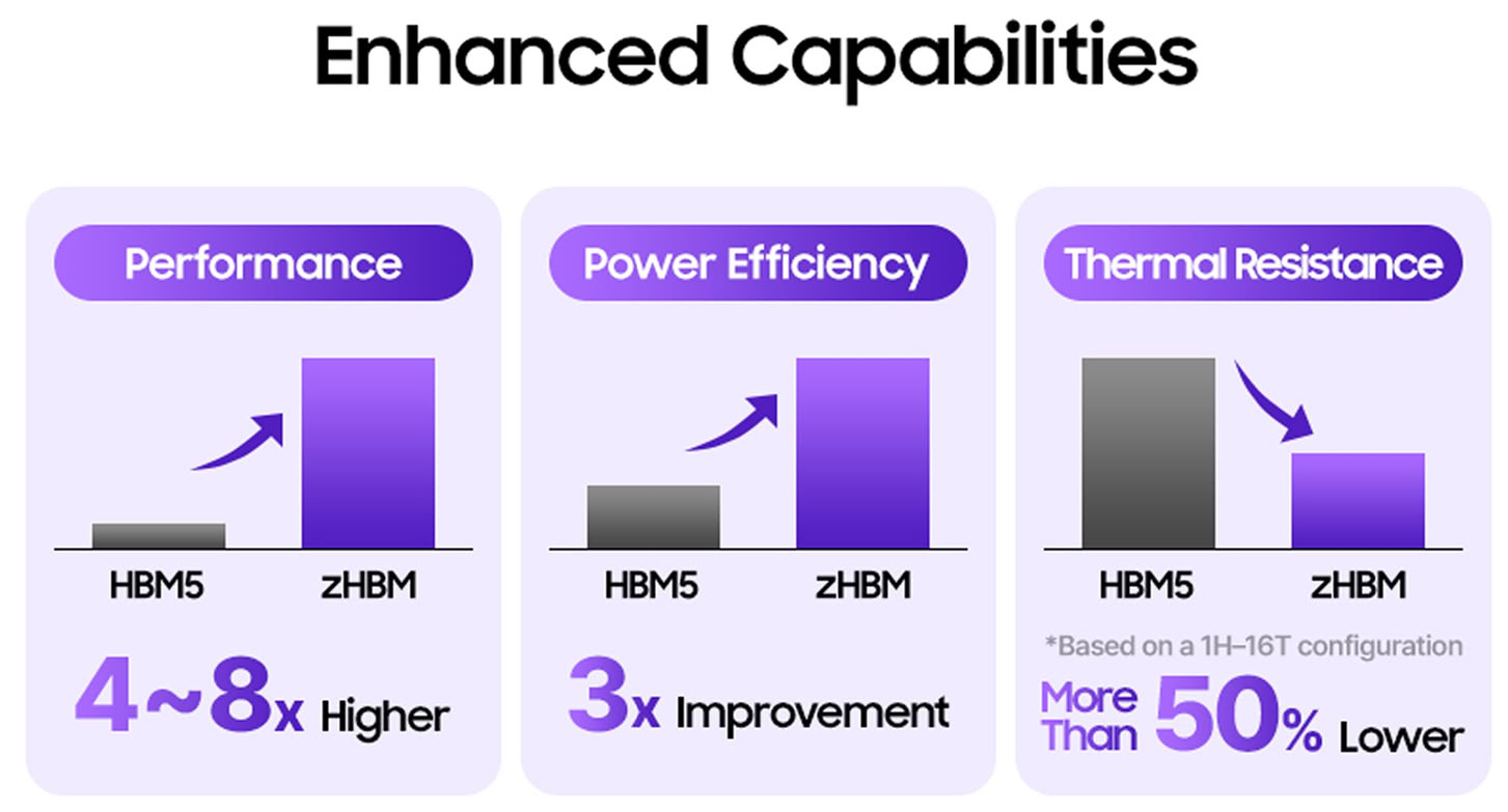
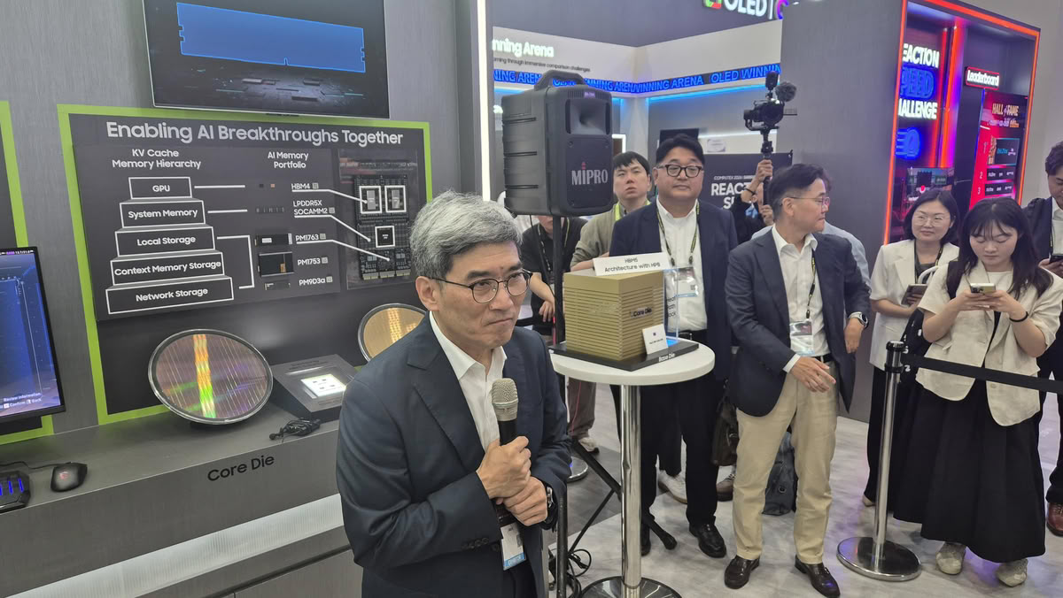
Samsung has demonstrated the industry's first zHBM concept products at FMS 2026, and this new architecture is expected to be launched after 2029. Redesigning the HBM architecture seems to have become the industry development direction. NVIDIA has also recently announced a customized NVHBM memory solution, which transfers the memory controller from the computing die to the HBM basic die.
In the NAND field, Samsung is developing zNAND-O for sample delivery in 2028. The product aims to achieve 10 times the bit density equivalent to DRAM while providing approximately 7 times the read bandwidth while maintaining the power efficiency of traditional NAND.
Competition faced by Samsung is also intensifying. In addition to SK Hynix, Chinese storage manufacturer Yangtze Memory has also recently put forward ambitious goals, planning to surpass Samsung and SK Hynix by the end of 2027.
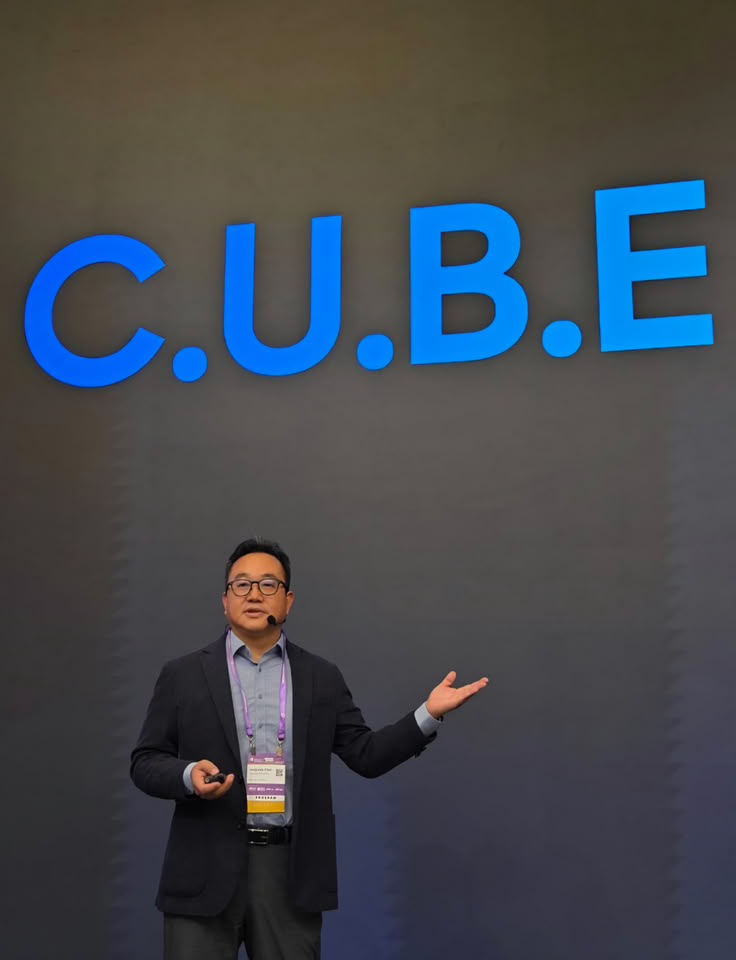
At the Memory Executive Summit held before the event, Samsung also introduced a memory development framework called "C.U.B.E", which stands for capacity, utilization, bandwidth and efficiency. The strategy includes increasing capacity without increasing PCB footprint by vertically expanding memory capacity; using optimized 3D architecture to reduce latency; using vertical high-speed channels to replace traditional horizontal data paths; and improving power consumption control and heat dissipation management from the bit level.
Comments