
Abstract:
Samsung Electronics has begun purchasing additional equipment for its wafer fab in Tyler, Texas, USA, with plans to further expand the production capacity of 2-nanometer process chips. According to industry news quoted by South Korean media ZDNet Korea, the equipment ordered by Samsung is expected to increase the production capacity of approximately 6,000 wafers per month. If subsequent equipment installation and production line construction proceed as planned, the monthly production capacity of Taylor Factory 1's 2-nanometer process is expected to reach 20,000 wafers in the second half of 2027.
The Taylor Wafer Fab is an important project for Samsung to lay out its advanced chip manufacturing business in the United States. Samsung announced the construction of an advanced process factory locally in 2021, with an initial announced investment of US$17 billion. The project aims to expand Samsung's advanced logic chip manufacturing capabilities in the United States while strengthening its competition with rivals such as TSMC in the global foundry market.
According to this report, Samsung has previously initiated the purchase and installation of relevant equipment, with the goal of establishing a production capacity of approximately 10,000 wafers per month. This new equipment order will further fill the unused space in the factory. In addition, Samsung also configured a trial production line in the early construction stage. If the trial production line and the previously planned production capacity are calculated together, Taylor Factory No. 1 is expected to gradually reach the design upper limit, which is to process 20,000 wafers per month.
The report pointed out that the installation and debugging of new equipment will be an important link for Samsung to achieve this goal. The capacity planning of the fab is not equivalent to the actual number of chips that can be delivered: after the equipment is in place, the company still needs to complete process debugging, yield improvement and customer verification before it can transform the design capacity into stable large-scale production capacity. Therefore, reaching a monthly output of 20,000 wafers in the second half of 2027 is still an expected goal, not an achieved result.
Samsung plans to use a 2-nanometer advanced process to produce logic chips at its Taylor Plant 1. As the requirements for chip performance and energy efficiency in fields such as artificial intelligence, high-performance computing, and autonomous driving continue to increase, advanced manufacturing processes have become an important competitive area for foundry companies to compete for high-value orders.
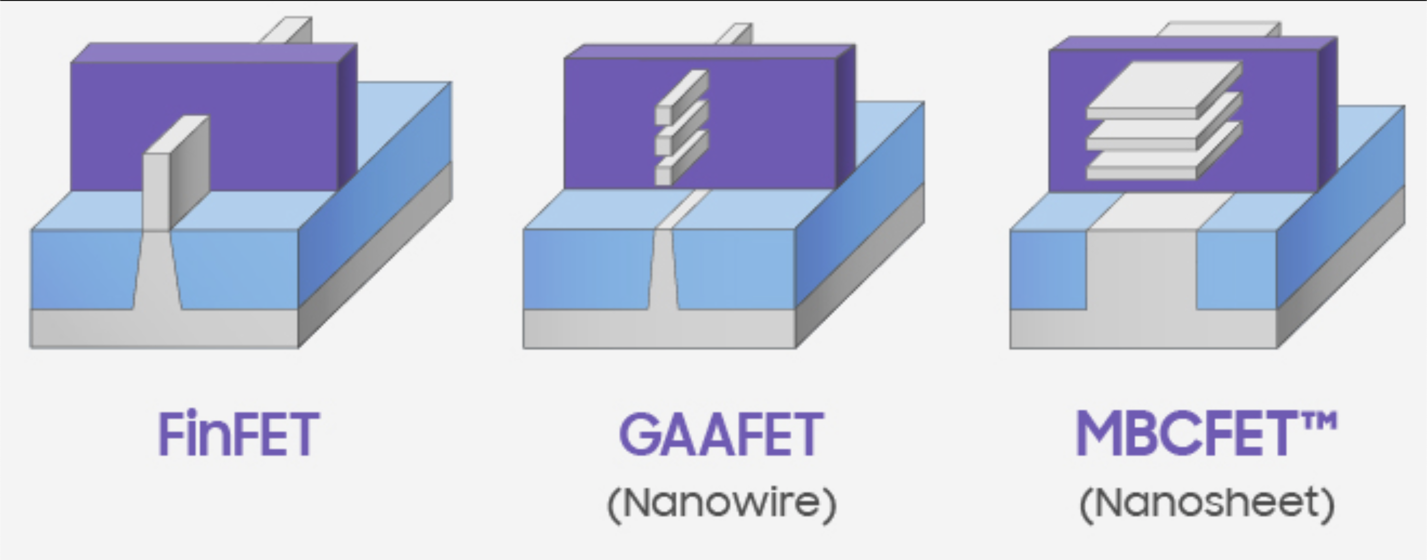
Samsung’s 2nm process uses all-around gate transistor technology (GAAFET), and the company calls its specific implementation MBCFET, which stands for multi-bridge channel field effect transistor. This structure enhances the ability to control current by allowing the gate to surround the transistor channel from multiple directions, helping to improve the operating characteristics of the transistor under low voltage conditions. Compared with traditional FinFET structures, GAAFET is regarded as an important technical direction for the continued shrinkage of advanced processes.
However, the process name does not directly represent the actual size of all structures in the chip, nor can it alone determine final performance. The energy efficiency, operating frequency, manufacturing cost and yield of the chip also depend on the transistor design, interconnect structure, process flow and design optimization of specific products.
In the global advanced wafer foundry market, Samsung still faces fierce competition from TSMC. TSMC has a strong customer base and mass production experience in the advanced process market, while Samsung needs to win more customer orders by improving process performance, increasing yields and stabilizing delivery capabilities. The advanced process production capacity in the United States has also become an important factor for customers when evaluating supply chain diversification.
Tesla is one of the important customers of Samsung’s advanced chip manufacturing business. Previous market news has linked the cooperation between the two parties to the demand for artificial intelligence chips, autonomous driving computing and other high-performance chips. If the Taylor factory can expand its 2-nanometer production capacity as planned, it will have the opportunity to provide more manufacturing resources for Samsung to undertake advanced chip orders in the United States. However, current public reports have not disclosed the specific customer orders corresponding to the new equipment and the proportion of production capacity occupied by each customer.
Samsung also plans to continue to expand the Taylor factory campus. According to information previously announced by the company, Taylor Plant II plans to start construction at the end of 2026 and aims to start operations in 2030. This means that Samsung is expanding its advanced logic chip manufacturing capabilities in the United States in stages, rather than relying solely on Taylor Factory 1 to meet future needs.
Samsung's wafer foundry business has faced profitability pressure in recent years. Capacity utilization, advanced process yield and customer order size are all important factors affecting operating performance. Expanding production capacity can create conditions for accepting more orders, but if customer demand is insufficient, or the yield rate and manufacturing cost of the new process cannot meet expectations, the new production capacity may not be quickly converted into profits.
In general, Samsung’s additional purchase of 2-nanometer equipment that can support the production of approximately 6,000 wafers per month is an important step in expanding the advanced process production capacity of Taylor Factory 1. According to the current plan, the factory is expected to reach the design capacity limit of 20,000 wafers per month in the second half of 2027. What will really determine the effectiveness of the project next will be the equipment installation progress, 2-nanometer process yield, customer order growth, and cost control capabilities after large-scale mass production.
Comments