
Abstract:
Samsung Electronics’ wafer foundry business finally ushered in an important breakthrough. According to South Korea's "Daily Economic News" reported on November 3, Samsung has received AMD's next-generation high-bandwidth memory (HBM) basic die order, and plans to use the second wafer fab (Taylor Fab 2) in Taylor, Texas, which is under construction in the United States, to produce related chips. According to reports, almost all of the planned production capacity of the factory has received customer orders, of which AMD accounts for the vast majority.
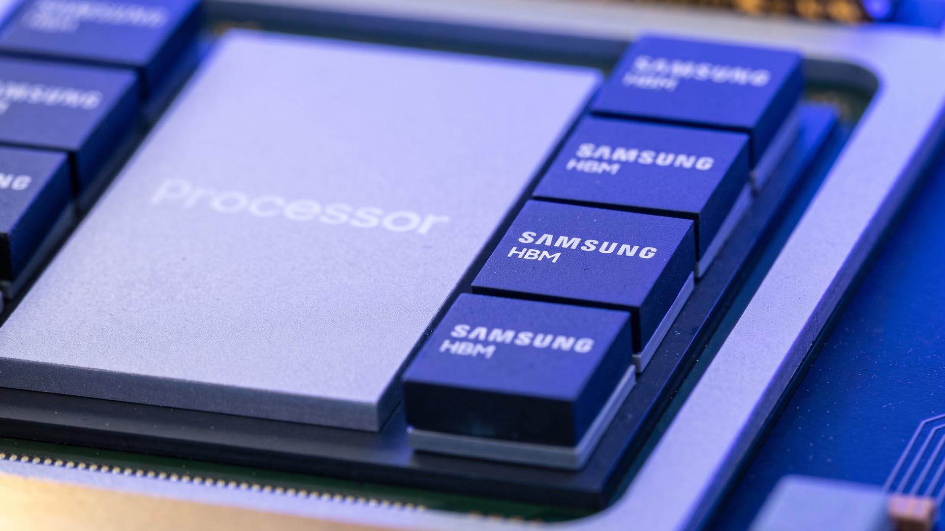
This order is of great significance to Samsung wafer foundry. In the past few years, Samsung has faced fierce competition from TSMC in the field of advanced processes, especially in the high-performance computing and artificial intelligence chip markets. It has always been difficult to obtain customer recognition equivalent to TSMC. The acquisition of AMD's HBM basic die order means that Samsung has the opportunity to combine its memory manufacturing advantages with advanced logic chip foundry capabilities to further expand its business scope in the AI hardware supply chain.
HBM is not simply stacking multiple DRAM chips together. The bottom usually contains a base die, which is responsible for managing the data transmission and control logic within the memory stack. As HBM technology continues to upgrade, the importance of the basic die is also increasing. Its design and manufacturing process will directly affect memory bandwidth, power consumption and overall performance.
Samsung plans to produce these basic die chips at its second factory in Tyler, and then ship them to South Korea for advanced packaging and stacking with DRAM chips produced at Samsung’s local memory factory to eventually form a complete HBM product. This division of labor can make full use of the respective production capabilities and technical resources of US wafer foundries and Korean memory manufacturing bases.
According to reports, Taylor’s second factory covers an area of approximately 2.7 million square feet, approximately 1.5 times the size of the first Taylor factory. Preparatory work for factory construction has been completed, and the main project is expected to be officially launched in November 2026. Samsung plans to start installing production equipment in February 2029 and achieve commercial mass production in 2030.
The factory is expected to use 2-nanometer and more advanced manufacturing processes to meet the performance and energy efficiency requirements of next-generation HBM for basic die. Different from traditional DRAM manufacturing, HBM basic die are logic chips and need to rely on advanced logic processes to achieve complex control functions. Therefore, they have become a new business area for wafer foundry companies to compete for.
It is worth noting that AMD is not the only customer that may use this factory. South Korean media reported that Samsung has received orders for the entire planned production capacity of the factory, and its customers also include Nvidia. However, AMD is currently said to occupy the vast majority of this capacity.
Nvidia’s situation is more complicated. Previously, it was reported that Nvidia hopes that memory suppliers such as Samsung, SK Hynix and Micron will uniformly manufacture the basic die of next-generation customized HBM products through TSMC to ensure that products from different suppliers use consistent manufacturing processes.
Nvidia is pushing for this standardization because different foundries may have differences in chip manufacturing processes, power consumption and thermal characteristics. If the basic die are manufactured by different manufacturers, Nvidia will need to invest more time in verification and adaptation. Unifying manufacturing by TSMC will help reduce performance differences between products from different suppliers and reduce the difficulty of developing the next generation of customized HBM.
This also means that even if Samsung obtains an AMD order, it may not immediately be able to achieve the same status in Nvidia's customized HBM supply chain. However, Samsung is still testing its own advanced wafer foundry process, hoping to prove that its technology can meet the requirements of next-generation products such as NVHBM. If Nvidia's demand exceeds the capacity that TSMC can provide in the future, Samsung may still have a chance to obtain additional orders.
For Samsung, the significance of the second Taylor factory is not only to obtain a large customer order, but also that its US wafer foundry business is gradually forming a scale. Previously, Samsung had secured orders for Tesla automotive chips for its first Taylor factory. Now there are reports of business progress related to AMD and NVIDIA, showing that it is working hard to win long-term cooperation with large American technology companies.
However, it should be noted that the current order mainly comes from industry news quoted by Korean media. Samsung officials have not yet confirmed specific customers and order allocation. Samsung only said it could not confirm customer-related information. Therefore, the size of AMD's order and whether Nvidia has confirmed the purchase should still be regarded as media reports rather than contract details officially announced by the company.
If the relevant plans are finally implemented, Samsung will have a large-scale advanced process factory dedicated to the new generation of HBM basic dies around 2030. This may not only help Samsung's wafer foundry business gain new growth momentum, but also mean that the competition in the AI chip industry chain in the future will no longer be limited to GPU and DRAM itself. HBM basic die and its manufacturing process will also become an important battlefield for semiconductor giants.
Comments