
Abstract:
Apple is about to hold a press conference on September 9, when it is expected to showcase its first iPhone chip A20 Pro, which is built using a 2-nanometer process. Previously exposed chip packaging information shows that Apple will switch from the old InFO_PoP solution to WMCM (wafer-level multi-chip module) technology. Now, the first front-side die photo of the A20 Pro has also leaked, showing a higher number of GPU cores and other improvements.
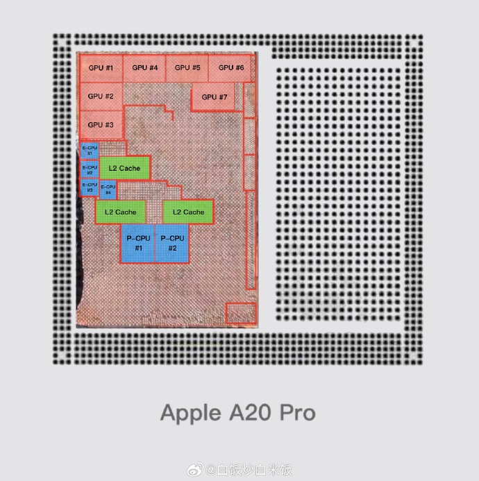
According to exposed information, the A20 Pro may become Apple's first iPhone system-on-chip equipped with a 7-core GPU, and use new packaging technology to bring stronger graphics performance. Previous A20 Pro news not only showed that it will use a new package, but also pointed out that the chip will be equipped with a larger-capacity neural engine, which is a further upgrade compared to the A19 Pro.
The photo was shared by Weibo user "白米饭吃白饭" and was later discovered by Reptalica and the relevant analysis was published on Notebookcheck.
A20 Pro is expected to be installed on iPhone 18 Pro and iPhone 18 Pro Max, and may also appear in Apple's first foldable flagship iPhone Fold. Existing information shows that the CPU configuration of the chip will not change and will still use two performance cores and four energy efficiency cores. The specific operating frequency has not yet been announced.
Apple seems to want to maintain the energy efficiency of the A20 Pro while improving performance, so it has not increased the number of CPU cores. Unlike competitors, Apple is still expected to continue to provide excellent single-core and multi-core performance through architectural optimization while maintaining the same number of cores. In terms of cache, the two performance cores are each equipped with 16MB L2 cache, which is consistent with the A19 Pro.
Changes are likely to occur primarily in the energy efficiency core. It is said that the A20 Pro’s energy-efficient core L2 cache will be increased from 6MB in the A19 Pro to 8MB. More importantly, the A20 Pro may be equipped with a 7-core GPU. Thanks to WMCM packaging, the memory die will be placed next to the SoC die instead of stacked on top of the SoC as in the past, which allows the memory bus width to be increased to 96 bits while continuing to adopt the LPDDR5X standard.
This design increases memory bandwidth without moving to the more expensive LPDDR6 standard. However, it is still not possible to judge the specific impact of this solution on energy efficiency. The relevant conclusions still need to wait until the first batch of A20 Pro running score data is released to confirm.
The currently exposed bare chip photos do not label modules such as neural engines or ISPs, so there are still a lot of chip details that have not been disclosed. As Apple’s launch event on September 9 approaches, more information is expected to be revealed.
Comments