
Abstract:
As demand for artificial intelligence and high-performance computing chips continues to explode, TSMC is accelerating the expansion of advanced process production capacity. The latest supply chain news shows that TSMC plans to further expand its 2-nanometer and 3-nanometer process production capacity in 2027. The expansion rate of 2-nanometer will be significantly higher than that of 3-nanometer. It is expected that by the middle of 2027, the monthly production capacity of 2-nanometer will increase to about 110,000 wafers, while the monthly production capacity of 3-nanometer will reach about 210,000 wafers.
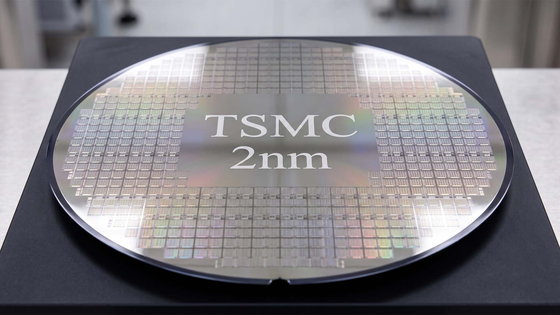
According to the current plan, TSMC’s 2-nanometer monthly production capacity by the end of 2026 is expected to be approximately 90,000 pieces, and its 3-nanometer monthly production capacity will reach approximately 180,000 pieces. By mid-2027, the production capacity of the two advanced processes will increase to 110,000 pieces and 210,000 pieces respectively. In comparison, the production capacity of 2nm will increase by approximately 22%, and that of 3nm will be approximately 16%.
This means that TSMC is significantly accelerating the ramp-up of its 2nm process capacity. Although 2nm is still a new generation process that has just entered the mass production stage, market demand has grown faster than 3nm, forcing TSMC to invest more resources to meet customer orders.
TSMC's 2-nanometer process has officially entered the high-volume production stage in the fourth quarter of 2025. The company has previously stated that the process has a good initial yield rate and is expected to achieve rapid production expansion in 2026. 2nm adopts a nanosheet transistor structure, which is an important node for TSMC to further promote the evolution of transistor architecture after FinFET.
Compared with the previous 3-nanometer process, one of the biggest technical changes in 2-nanometer is the shift from FinFET to GAA, which is a surround-gate transistor structure. By having the gate more fully surround the channel, the transistor's ability to control current flow can be further improved and a better balance between performance, power consumption and transistor density can be achieved.
Currently, 2nm has become one of TSMC’s most important advanced processes in the next few years. Apple is considered to be one of the first major customers to adopt TSMC's 2-nanometer process. The high-end chips used in the new generation of iPhones have already entered this process era. As other large chip design companies besides Apple gradually shift to 2nm, TSMC is expected to face increasing pressure on production capacity.
AI chip demand is another key factor driving the expansion of advanced process production capacity. In recent years, NVIDIA, AMD and other AI chip manufacturers have continued to launch more complex accelerators and high-performance computing products. These products require the use of the most advanced manufacturing processes to improve computing performance while reducing energy consumption per unit of computing power.
Compared with 3nm, the capacity scale of 2nm is still smaller at present, but TSMC obviously hopes to expand it as soon as possible to a level sufficient to take on more customers. According to the current plan, the monthly production capacity of 2nm will reach 110,000 pieces by mid-2027. Although this number is still lower than the 210,000 pieces of 3nm, the gap between the two has begun to narrow.
At the same time, TSMC has not slowed down its 3-nanometer production expansion. It is expected that by mid-2027, the monthly 3-nanometer production capacity will reach approximately 210,000 pieces. TSMC is expanding 3-nanometer manufacturing capabilities at multiple production bases in Taiwan and outside Taiwan. Among them, the second wafer fab in Arizona, the United States, also plans to adopt the 3-nanometer process and is expected to start mass production in the second half of 2027.
TSMC’s production base in southern Taiwan is also adding 3nm production capacity. The company has previously announced that it will add a new 3-nanometer wafer fab in the Tainan Science Park and is expected to enter mass production in the first half of 2027. In addition, Japan’s second wafer fab in Kumamoto also plans to use the 3-nanometer process and is expected to start mass production in 2028.
The advanced process layout in Arizona, USA, is an important part of TSMC's global production strategy. In addition to the first fab that has started production, the construction of the second fab has also been completed, and it is planned to start 3nm mass production in the second half of 2027. This will further expand TSMC's 3nm supply capabilities and allow some advanced chip production to be completed directly in the United States.
In order to further expand 3nm production capacity, TSMC is also adjusting some existing production equipment in Taiwan and converting equipment originally used for the 5nm process to 3nm production. In this way, TSMC can increase its output of advanced process wafers faster without relying entirely on new fabs.
This capacity adjustment also reflects the changing demand structure of the chip market. The growth of the smartphone market has slowed down in the past few years, and the demand for mature processes for some entry-level and mid-range mobile phone chips has declined, while AI, high-performance computing, and high-end smartphones have continued to increase the demand for advanced processes. Therefore, converting some old process equipment to more advanced nodes can improve the resource utilization efficiency of the entire production system.
TSMC is currently facing not only pressure on wafer manufacturing capacity, but advanced packaging has also become an important link restricting the supply of AI chips. As AI accelerators require large-scale integration with HBM high-bandwidth memory, the demand for advanced packaging technologies such as CoWoS has grown rapidly in recent years. TSMC is also continuing to expand its advanced packaging production capacity to avoid being limited by the packaging process after increasing its wafer manufacturing capacity.
In the next few years, TSMC’s advanced process route will continue to advance to smaller nodes. The company has begun to promote the 1.4-nanometer A14 process and plans to achieve mass production in 2028. Recent supply chain news has even spread that TSMC may further advance the trial production and mass production time of the 1.4nm process, but the specific timetable still depends on the progress of fab construction and process development.
At the same time, 2nm itself will not stay at the initial version. TSMC has planned 2nm derivative processes such as N2P and further launched A16. N2P will further improve performance and power consumption based on the original N2, while A16 introduces TSMC's Super Power Rail back-side power supply technology, which is more suitable for high-performance computing and chips with complex signal paths and high power supply density.
From the perspective of the entire industry trend, TSMC is currently forming a continuous advanced process echelon consisting of 3 nanometers, 2 nanometers and 1.4 nanometers in the future. 3nm will continue to undertake large-scale advanced chip production tasks in the next few years, while 2nm will gradually become the core manufacturing node for flagship smartphone processors, AI accelerators and high-performance computing chips.
The growth rate of 2nm production capacity exceeds that of 3nm, which also shows that TSMC is reallocating capital and manufacturing resources according to market demand. It is expected that by 2027, as the 2nm yield rate continues to improve and more customer products enter mass production, the proportion of production capacity of this process will further increase.
If the current expansion plan is implemented smoothly, TSMC will have a monthly production capacity of approximately 110,000 2nm wafers and 210,000 3nm wafers by mid-2027. For the global semiconductor industry, which is experiencing a boom in AI infrastructure construction, this will significantly expand the supply scale of the most advanced logic chips and further consolidate TSMC's leading position in advanced process manufacturing.
Comments