
Abstract:
The advancement speed of TSMC’s next-generation 1.4nm process may once again exceed market expectations. According to the latest reports from Taiwanese media, TSMC’s 1.4nm wafer fab in Taichung is expected to start trial production in April 2027 and enter mass production in the second half of 2027. If this timetable is finally realized, it will be about one year ahead of TSMC's previously announced mass production plan for 2028, which also means that competition for the world's most advanced logic processes will further accelerate.
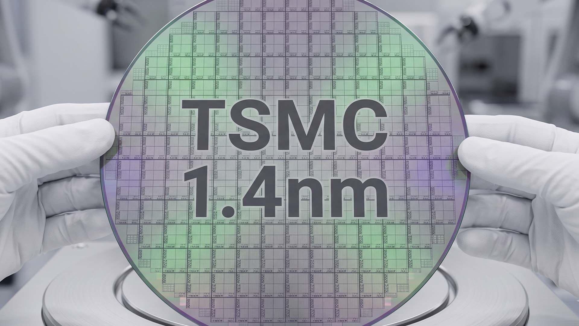
TSMC’s 1.4nm process is called A14, which is the next generation of advanced process after 2nm N2. TSMC has previously made it clear that the A14 was originally planned to enter mass production in 2028. The current development is progressing smoothly, and the research and development and yield performance of related technologies are ahead of the company's previous expectations. TSMC reconfirmed at its first quarter financial report meeting in 2026 that the A14 mass production schedule is still set in 2028.
However, the latest news shows that the construction speed of the A14 production base in Taichung has been significantly faster than the original plan. The project will start construction in October 2025. Currently, the entire park is planning to build four 1.4 nanometer wafer fabs. The first factory building has completed the steel structure construction and is undergoing floor, wall and other building construction. It is expected to be completed in early 2027.
If construction continues at the current pace, trial production of the first plant may begin in April 2027. Subsequently, with equipment installation, production line verification and process certification proceeding smoothly, mass production is expected to start in the second half of 2027. This means that TSMC may advance A14 from the factory construction stage to real commercial production in less than two years.
The second factory building has completed the foundation concrete construction and is entering the steel structure construction stage, which is expected to be completed around October 2027. According to the current plan, both the first and second factories are expected to begin undertaking 1.4nm process production tasks in 2027. The third factory has obtained the construction permit, and the fourth factory is still going through relevant procedures. The construction of the two factories is expected to be completed in 2028.
Previously, in July this year, TSMC reported that it might start 1.4nm trial production in advance in the third quarter of 2027. At that time, the market expected that large-scale mass production might still have to wait until after mid-2028. Now the latest reports have further advanced the trial production time to April 2027, showing that TSMC is continuing to compress the A14 promotion cycle.
The investment scale of this 1.4nm production base located in the Central Taichung Science Park is also quite large. According to reports, TSMC plans to invest approximately US$49 billion in building related facilities. Such a huge investment will not only be used in the wafer fab itself, but will also drive peripheral semiconductor equipment, factory engineering, clean rooms and material suppliers to further expand their presence in Taichung.
TSMC is currently at a critical stage of competition in advanced manufacturing processes. Its 2-nanometer N2 process has entered the mass production stage, and A14 is an important node further moving towards the "Ami Era". Compared with N2, TSMC's official A14 specifications show that the performance can be improved by up to 15% under the same power consumption, or the power consumption can be reduced by up to 30% under the same performance, while the chip logic density is increased by more than 20%.
A14 adopts the second-generation nanosheet transistor structure and cooperates with TSMC’s NanoFlex Pro technology. Compared with traditional transistor structures, this architecture can further improve the performance and energy efficiency of transistors, and provide a more advanced manufacturing basis for products that are extremely sensitive to computing power and energy consumption, such as smartphones, artificial intelligence, and high-performance computing.
TSMC also revealed in this year’s financial report meeting that A14’s current customer interest is very high, with customers actively participating in the two major fields of smartphones and high-performance computing. The company stated that the technical development progress of A14 is in good progress, and its performance and yield indicators are advancing as planned. As the demand for artificial intelligence chips continues to explode, A14 is likely to not only be used in flagship mobile phone processors in the future, but will also become an important manufacturing platform for next-generation AI accelerators and high-performance computing chips.
At the same time, competition in advanced manufacturing processes is also entering a more intense stage. Intel currently plans to use the 14A process for risk trial production of internal products in the second half of 2027, and enter high-volume manufacturing in 2028. Samsung is re-promoting the 1.4nm SF1.4 process, with mass production expected to be around 2029. If TSMC can achieve A14 mass production in the second half of 2027 according to the latest schedule, its time advantage will be further expanded.
TSMC’s progress on A14 is also related to the current huge demand for advanced wafer production capacity in the artificial intelligence industry. Products including AI accelerators, data center processors and high-end mobile phone chips are promoting the continuous migration of wafer factories to more advanced process nodes. For TSMC, the sooner it completes A14 mass production, the more likely it is to lock in customers and production capacity before the next round of AI chip manufacturing demand explodes.
However, it should be noted that April 2027 is still the trial production time reported by the media and is not TSMC’s officially confirmed mass production commitment. There are still multiple stages in the process from factory completion to equipment installation, process verification, yield ramping, and finally reaching large-scale commercial production capabilities. Therefore, even if the construction of the first factory building can be completed on schedule, whether A14 can ultimately achieve stable mass production in the second half of 2027 still depends on equipment installation, process maturity, and yield improvement speed.
If the latest timetable eventually becomes reality, TSMC will significantly advance the commercialization time of the 1.4nm advanced process from the original 2028 to 2027, and further consolidate its leading position in the global advanced wafer foundry market. For TSMC, Intel and Samsung, which are competing for orders for next-generation AI chips, 1.4nm is no longer just a future node on the technology roadmap, but is quickly becoming a key battlefield that will determine the competitive landscape of advanced chip manufacturing in the next few years.
Comments