
Abstract:
Samsung and Qualcomm are further expanding the scope of cooperation in the semiconductor field. The two parties have already cooperated on 2.1D advanced packaging technology, with the goal of providing higher-density and higher-speed chip interconnect solutions for the next generation of high-performance computing and artificial intelligence chips. This cooperation is also seen as an important step for Samsung to further improve its advanced packaging technology system and compete for the AI chip packaging market.
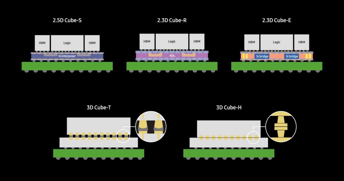
With the development of generative AI and high-performance computing, the amount of data that a single chip needs to process continues to increase, and traditional packaging methods are increasingly difficult to meet the needs of high-speed and large-scale data transmission between chips. In particular, AI accelerators usually need to integrate computing chips with high-bandwidth memory and other functional chips in the same package. Therefore, advanced packaging has become an important link affecting the performance of AI chips.
One of the most mainstream high-end solutions in the industry currently is 2.5D packaging. This approach typically connects multiple chips through a silicon interposer, enabling very high-density signal interconnections between chips. However, the cost of the silicon interposer itself is relatively high, and as the package size continues to expand, its manufacturing difficulty and yield pressure will further increase.
2.1D packaging attempts to achieve a new balance between performance and cost. Its core feature is that it no longer relies on traditional silicon interposers, but uses high-density fine lines on advanced packaging substrates to directly connect different chips. The 2.1D packaging substrate recently demonstrated by Samsung uses this idea to achieve high-performance chip interconnection without using a silicon interposer through thinner lines and higher-density connection structures.
For AI accelerators, this solution has certain appeal. AI chips often need to transmit massive amounts of data between computing chips, high-performance memories such as HBM, and other chips. The interconnection speed and bandwidth within the package directly affect the performance of the entire system. If the cost of the interposer can be reduced through 2.1D technology while maintaining a high enough interconnect density, it may become an alternative for some AI and high-performance computing products.
Samsung is currently actively expanding its layout of 2.1D and 2.5D packaging technologies. Samsung Electro-Mechanics recently demonstrated 2.5D and 2.1D packaging substrates for AI accelerators. The 2.5D solution focuses on solving the warpage problem of large-size, high-rise substrates and improving high-speed signal transmission and high-density connection capabilities; the 2.1D solution focuses on using fine lines and high-density connection technology to achieve direct connections between chips without a silicon interposer.
This shows that Samsung is trying to establish a complete set of AI chip solutions from wafer manufacturing, memory to advanced packaging substrates. Samsung Electronics has currently established the Multi-Die Integration Alliance, which provides a complete technical system from chip design to packaging and testing for multi-chip integration by cooperating with EDA, IP, DSP and packaging and testing companies.
Samsung's advantage is that it is not just a foundry company, but also has the world's leading memory business and advanced packaging capabilities. AI accelerators increasingly rely on HBM, and Samsung can not only produce logic chips, but also provide HBM and advanced packaging, so it can theoretically provide customers with a more complete supply chain solution.
Qualcomm has a lot of experience in chip design for high-performance mobile SoCs and other computing platforms. The two parties have maintained a long-term cooperative relationship in the past, and Qualcomm's Snapdragon chips were also produced using Samsung's foundry technology. In recent years, the two companies have further expanded their cooperation in the fields of mobile chips, Galaxy devices and artificial intelligence.
This further expansion of the scope of cooperation to 2.1D advanced packaging also means that Qualcomm can use Samsung's technical capabilities in packaging substrates and advanced packaging to explore more complex multi-chip integration solutions in the future.
For Qualcomm, the importance of advanced packaging is also rising. As mobile phones, PCs, and edge AI devices increasingly run large-scale AI models, a single SoC needs to integrate more and more computing units, caches, NPUs, and high-speed storage resources. Combining multiple chips together through chiplets and advanced packaging technology can avoid continuing to rely solely on expanding the size of a single chip to improve performance.
This change is also consistent with the development trend of the entire semiconductor industry. As advanced manufacturing processes continue to approach physical limits, the cost and performance benefits of continuing to shrink transistor sizes are gradually decreasing. Therefore, the industry has begun to rely more on technologies such as chiplets, 2.5D, 3D packaging, and high-bandwidth memory to achieve performance improvements through system-level integration.
Samsung is currently not only increasing investment in the 2.1D and 2.5D fields, but also advancing glass substrate technology. Glass offers greater rigidity and dimensional stability than traditional organic material substrates, and has the potential to improve performance such as signal transmission, power integrity and heat dissipation. As the size of AI chip packaging continues to expand, glass substrates are considered to be one of the important technologies for the next generation of large-size advanced packaging.
At the same time, Samsung is also developing 3D packaging technology, including X-Cube and other solutions. By vertically stacking chips, the data transmission distance between chips can be further shortened and the interconnection density per unit area can be significantly increased. For AI and high-performance computing, this type of technology may form Samsung's complete advanced packaging technology portfolio together with 2.1D and 2.5D packaging in the future.
The significance of this 2.1D packaging cooperation between Samsung and Qualcomm is not just to launch a new packaging form, but more importantly, the two parties are jointly exploring chip integration methods in the post-Moore era. Future high-performance chips may no longer be a single chip of increasing size, but a highly integrated computing system composed of CPU, GPU, NPU, cache, HBM and other dedicated cores.
In this process, the importance of the packaging substrate will become closer and closer to the chip itself. How high the bandwidth can communicate between chips, whether stable signal quality can be maintained, how large the package size can be, and the manufacturing cost and yield rate of the entire package may directly determine the final market competitiveness of an AI chip.
This cooperation between Samsung and Qualcomm will also give Samsung further opportunities to compete with TSMC’s advanced packaging system. At present, the AI chip market largely adopts 2.5D advanced packaging based on technologies such as CoWoS, and Samsung is establishing its own alternatives through multiple technical routes such as 2.1D, 2.5D, 3D, and glass substrates.
If 2.1D technology can achieve sufficiently high interconnect density and bandwidth in actual products while reducing reliance on expensive silicon interposers, it is expected to become an important packaging option for future AI accelerators, data center processors, and other high-performance chips. This cooperation between Samsung and Qualcomm may also become an important technical foundation for both parties to further enter the AI infrastructure market.
Comments