Samsung announced that it has delivered samples of its new generation HBM4 memory to global customers and is expected to achieve mass production in 2026. Samsung confirmed in its just-announced third quarter 2025 performance report that HBM3E has now entered mass production and been sold to relevant customers, while HBM4 samples have also been sent to key customers simultaneously. Samsung said that its storage business is still performing strongly and the market demand for advanced memory products is strong.
In addition, Samsung also revealed that its wafer foundry business will be committed to stably supplying new 2-nanometer GAA products and HBM4 basic chips in 2026, and plans to put its new factory in Tyler, Texas, into operation on time.
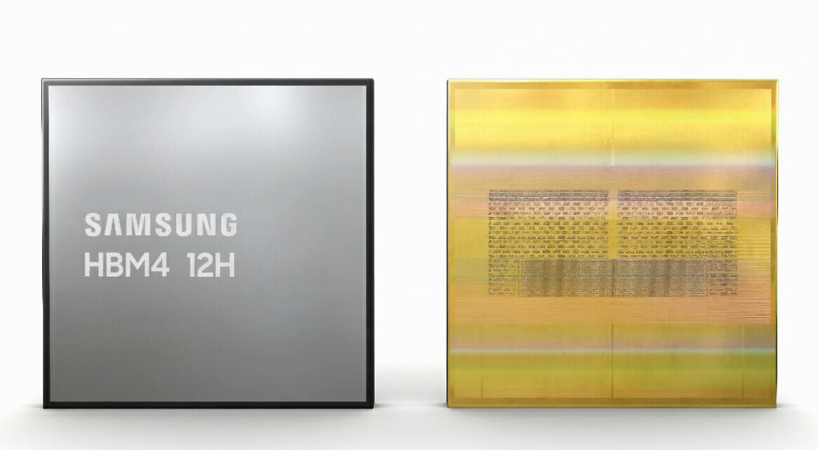
The HBM stack consists of up to 12 layers of stacked DRAM chips connected by through silicon vias (TSVs), with optional embedded base chips providing custom logic or acceleration circuits to meet special needs. Usually, large customers such as NVIDIA and AMD require customized functions due to large purchase volumes. Although these chips do not necessarily have powerful computing capabilities, data processing and logic chips can improve packet transmission efficiency, reduce latency, and enhance the performance of the inference stage, significantly improving throughput.
According to reports, it is still unclear whether Samsung HBM4 will go beyond the JEDEC standard to meet the needs of companies such as NVIDIA. For example, Micron has skipped the JEDEC specification and increased the bandwidth of HBM4 from the standard 2 TB/s and 8 Gb/s per pin to 11 Gb/s, increasing the total bandwidth to 2.8 TB/s, which is 40% higher than the standard. Therefore, it is expected that Samsung will continue to optimize its HBM4 to maintain market competitiveness in aspects such as bandwidth and better meet the needs of large customers.