Guo officially launched two mobile processors, A19 Pro and A19, three months ago. They continue to use the 3-nanometer, 64-bit Arm architecture and become the core platform for the new generation iPhone 17 series and the ultra-thin and lightweight iPhone Air. As independent institutions successively released high-magnification wafer photos of A19 Pro in mid-November, the industry was finally able to conduct a detailed comparison of its layout, and focused its analysis on the application effects of TSMC's latest N3P process node.
Compared with the previous generation A18 series, which is also 3 nanometers but based on the N3E FinFET process, N3P is positioned as a "high-performance variant" and can theoretically bring a certain degree of area and energy efficiency advantages.
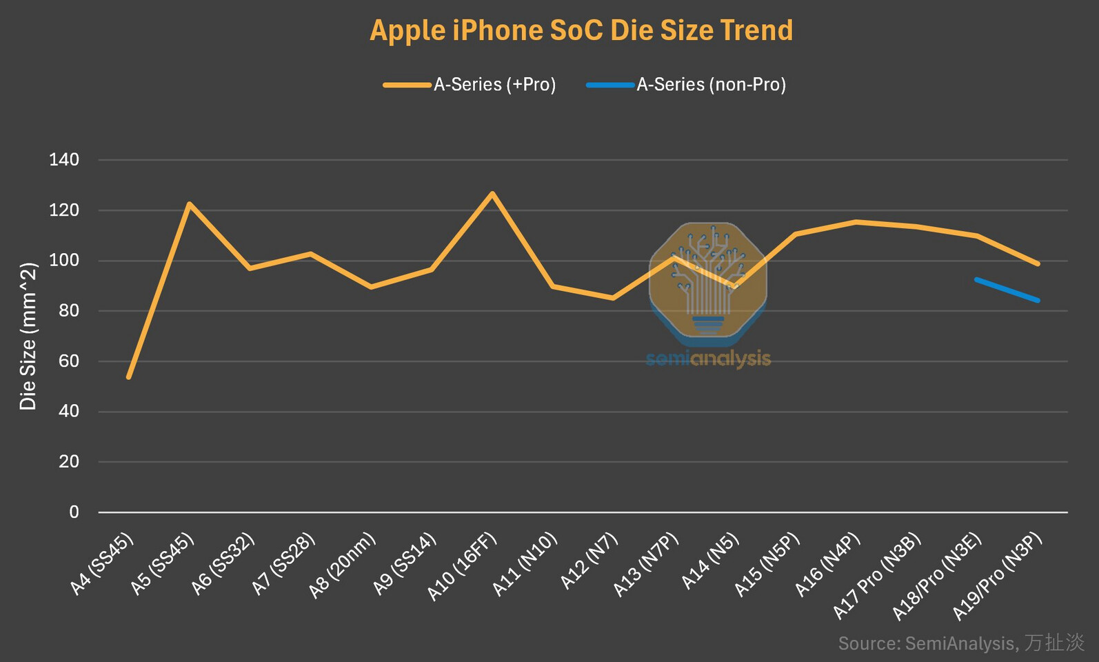
Judging from specific data, the package area of the current flagship A19 Pro has been reduced by about 10% compared to the A18 Pro, from 105 square millimeters to 98.6 square millimeters; while the standard version of the A19 has also been reduced by about 9% compared to the previous generation A18. SemiAnalysis, a semiconductor analysis organization, estimates that the process evolution from N3E to N3P alone can theoretically only contribute about 4% to the area reduction, which means that Apple has made additional and larger optimization adjustments at the architecture and layout levels.
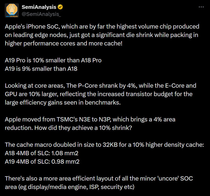
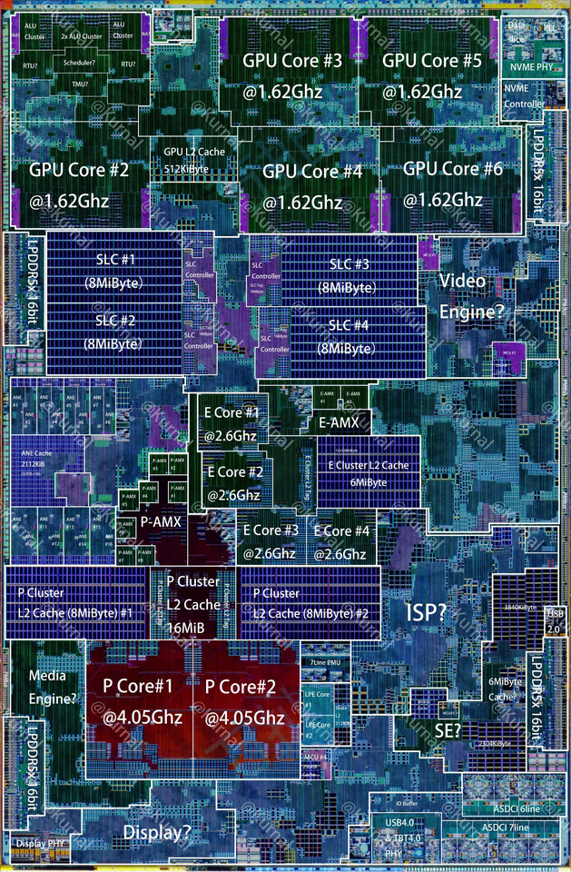
In terms of core and cache configuration, analysis points out that the performance core (P-Core) area has shrunk slightly, by about 4%, while the energy efficiency core (E-Core) and GPU area have increased by about 10%, reflecting Apple's design orientation of tilting more transistor resources to improve energy efficiency and graphics performance under the same packaging area budget. In addition, the cache macrocell capacity is doubled to 32 KB, while achieving a density increase of about 10%: with the same 4 MB SLC (system level cache), the A18 corresponds to an area of about 1.08 square millimeters, while the A19 is only about 0.98 square millimeters.
In addition to the core and cache, the A19 series also adopts a more efficient layout in the so-called "uncore" SoC area (including display/multimedia engine, image signal processor ISP, security module, etc.) to further compress the area ratio of non-computing units. Comprehensive process upgrades, core block reallocation and peripheral module layout optimization, SemiAnalysis evaluation believes that the 9%-10% reduction in the overall packaging area of the A19 Pro series is close to a space saving effect "equivalent to a large node jump", and can be regarded as a representative achievement of Apple's tapping of potential through the architecture and design level on the existing 3nm platform.