The physical image of Huawei's new generation Ascend 950 AI accelerator has been exposed for the first time, showing the packaging form of the company's self-developed chip and self-developed high-bandwidth memory (HBM). This chip integrates Huawei's first-generation self-developed HBM and a new generation of AI acceleration units in the same package. It is positioned for large-scale computing clusters and competes through system scale and cluster density, rather than "hard-core" rivals such as Nvidia in terms of performance of a single chip.
Huawei has previously announced that the Ascend 950 series is scheduled to be officially launched in early 2026 and will include at least two models.
Reports show that among the Ascend 950 series, the 950PR version integrates 128 GB Huawei’s self-developed HBM, with a bandwidth of approximately 1.6 TB/s; while the 950DT version increases the capacity to 144 GB and significantly increases the bandwidth to nearly 4 TB/s. The computing power targets of both chips are 1 PetaFLOPS level FP8 performance and 2 PetaFLOPS level FP4 performance for a single card, targeting current mainstream large model inference and training scenarios. Huawei's overall strategy puts more emphasis on high-density packaging and efficient interconnection networks, and offsets the gap in single-chip performance by improving computing power and interconnection efficiency at the cabinet and data center levels.
In terms of manufacturing process, the article points out that there is currently no officially confirmed process node information, but the industry generally expects that the Ascend 950 is likely to use SMIC's latest N+3 process, which is classified as a 5 nm node. SMIC has previously announced that its N+3 node has achieved mass production without relying on EUV equipment, and the first public customer is Huawei's terminal product equipped with Kirin 9030 SoC. In this context, as Huawei's strategic AI acceleration product, it is considered a "natural" inference that Ascend 950 uses the same node.
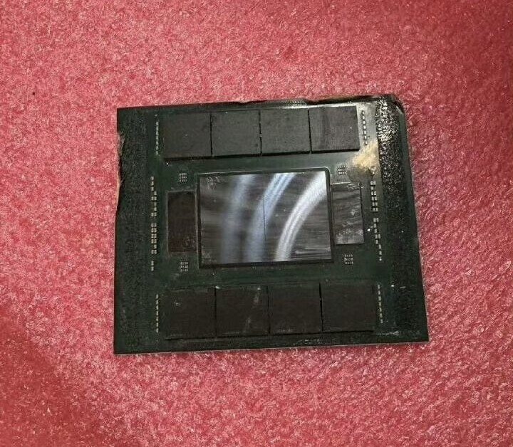
From the physical picture, the Ascend 950 adopts a multi-chip packaging design. The core is two computing chip dies, and is paired with two additional suspected I/O and network-related chip dies to form a multi-chip module (MCM). These I/O and network chips are believed to be responsible for connecting accelerator cards to larger SuperPoD and SuperCluster clusters, achieving high-bandwidth interconnection of hundreds of thousands of Ascend 950 cards through a new generation of "Lingqu" interconnection protocol and optical interconnection technology. The module with a ring of packaging structure distributed around the die that looks similar to the "LPDDR/HBM hybrid form" is speculated to be Huawei's self-developed HBM package. It is most likely produced in an independent package and then stacked and integrated on the accelerator substrate in a system-level package.
Overall, the design route of Ascend 950 has some similarities with high-end GPUs such as NVIDIA Blackwell. Both use dual-chip packaging to superimpose more computing power on a single card, and rely on high-bandwidth HBM and dedicated interconnect protocols to build large-scale computing clusters. The difference is that Huawei is more focused on the idea of "winning by scale" at the current stage, hoping to form alternative solutions in the data center and AI cloud computing power markets through dense packaging, multi-card interconnection and super cluster solutions, while strengthening the independent controllability of the local supply chain.