At the recent J.P. Morgan Global Technology, Media and Communications Conference, Intel CEO Lip-BuTan announced a series of strong internal reform measures and an advanced process roadmap. He made it clear thatThe most stringent quality control policy will be implemented for the wafer foundry business. If any product fails to meet mass production standards within the specified steps, the relevant person in charge will be fired directly.
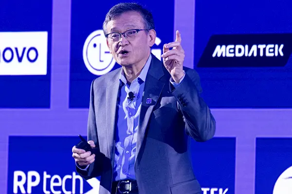
Chen Liwu revealed,Intel has long had the problem of being unable to mass-produce its products after multiple iterations. Many chips need to go through multiple steps above B0 before they can be finally launched on the market. This has not only led to serious delivery delays, but has even led to the direct cancellation of multiple core projects.To this end, he has officially implemented the iron law of "A0 to production".
What needs to be explained here is that chip stepping (Stepping) refers to the version iteration number of the chip from design to mass production. Each step corresponds to a complete design revision and tape-out, which is mainly used to repair hardware bugs, optimize performance or improve yield. in:
A0 step: It is the initial version that is taped out for the first time after the chip design is completed. It is equivalent to an engineering prototype. It usually has many undiscovered design defects and can rarely be directly mass-produced.
B0 step:It is the first comprehensive revision of the A0 version problems. In theory, it should solve all fatal bugs and reach mass production quality standards.
Each additional step (such as C0, D0) means an additional 3-6 months of research and development cycle and tens of millions of dollars in tape-out costs. This is also one of the core reasons why Intel's products have frequently been delayed in the past ten years and its competitiveness has declined.Chen Liwu's new rules directly cut off this escape route: "You can still keep your job at B0. If you make any progress beyond B0, you will be fired."
He emphasized,At first many employees thought he was joking, but now everyone understands the seriousness of the policy, and teams are working hard to ensure all issues are resolved within the stipulated time.
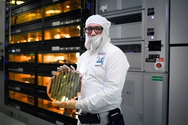
In terms of advanced processes, Chen Liwu confirmed that the 14A (1.4nm) process is advancing as planned, and will start risk mass production in 2028 and achieve large-scale mass production in 2029. This time node is completely synchronized with TSMC's A14 process.
At present, Intel has started negotiations with major customers such as Apple and TeraFab. The 0.5 version process design kit (PDK) of the 14A process has been delivered to external customers at the beginning of this year. The 0.9 version PDK is planned to be officially released in October 2026, and internal customers will obtain the right to use it earlier.
At the same time, Intel has launched long-term research and development plans for 10A (1.0nm) and 7A (0.7nm) processes, forming direct competition with TSMC.
Chen Liwu pointed out that when customers choose a foundry, they not only value the performance of a single node, but also pay more attention to the complete long-term technology roadmap. In addition to advanced processes, Intel also maintains leadership in advanced packaging technologies such as EMIB, and plans to launch glass substrate solutions in 2030. Driven by the AI super cycle, the current supply of Intel substrates is extremely tight, and many customers have paid advance payments in advance to lock in production capacity.
Industry analysts believe that Chen Liwu's iron-fisted reforms will reshape Intel's credibility in the wafer foundry field, regain the trust of customers through strict quality control and a clear technology roadmap, and challenge TSMC's industry dominance.