Recently, photos of the inside of the chip of Samsung's Exynos 2600 application processor leaked out. After being marked by Kurnal Salts, they showed that this processor designed for smartphones, tablets and ultra-portable notebooks has a large-scale complex logic circuit structure and integrates a large number of on-chip memory and computing units. The chip is produced using Samsung's self-developed SF2 process technology, a 2-nanometer GAAFET process node whose transistor density and electrical performance are comparable to TSMC's N2 process. The entire chip is a monolithic design, with all logic components integrated on the same chip.
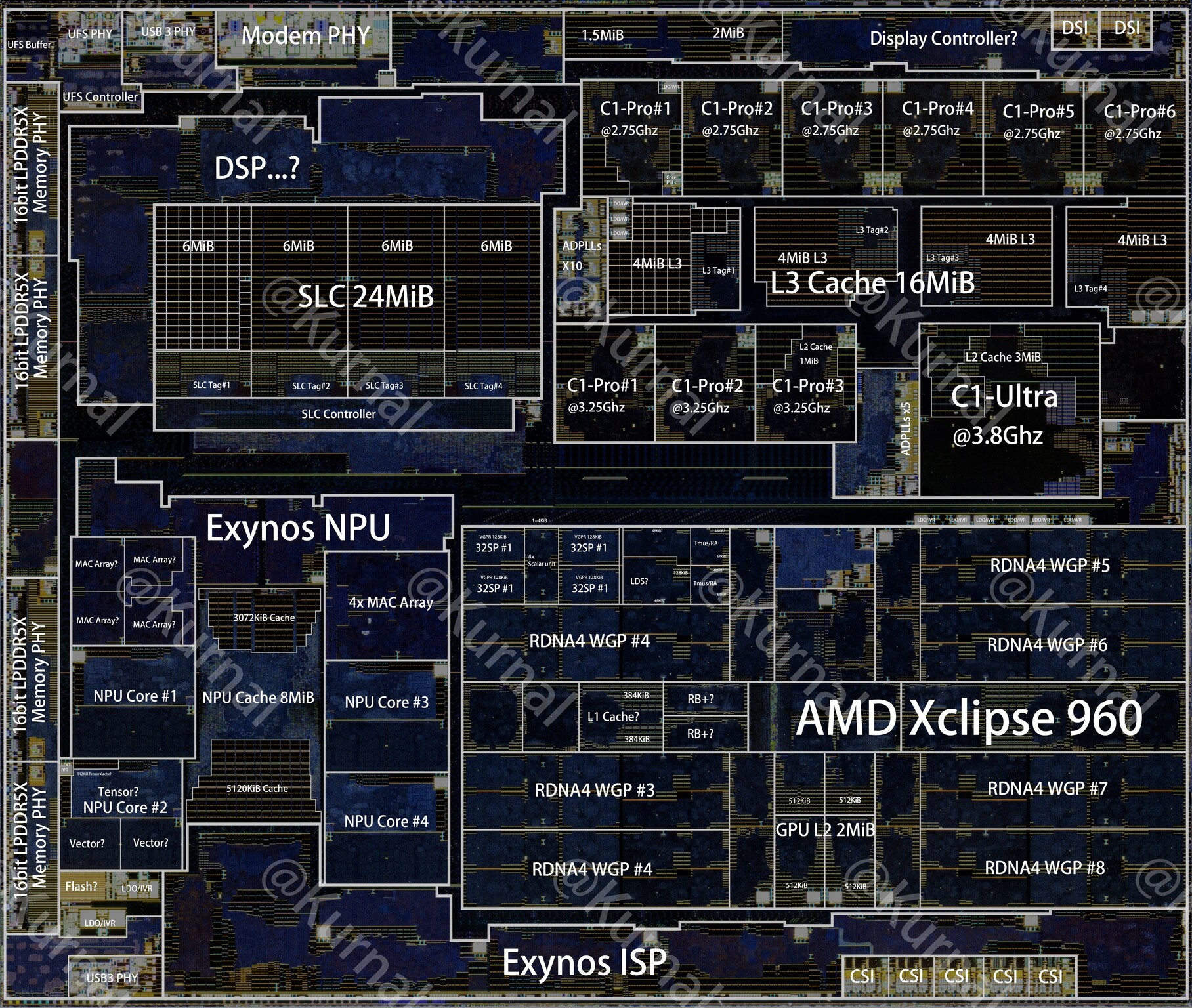
In terms of processor core, Samsung designed a three-layer heterogeneous multi-core architecture for the Exynos 2600, using a configuration mode of 1 ultra-large core + 3 performance cores + 6 energy efficiency cores. One of the C1-Ultra ultra-large cores is clocked at 3.80 GHz, providing the highest single-core performance and equipped with a 3 MB dedicated L2 cache. Followed by three C1-Pro performance cores, running at a maximum frequency of 3.25 GHz, used to handle most high-performance load tasks, each core has a 1 MB dedicated L2 cache. The other six cores, which are also based on the C1-Pro architecture, are set as energy-efficiency cores, with a main frequency of only 2.75 GHz and a more radical power management strategy. It is worth noting that the performance core and energy efficiency core on this chip are functionally identical, and the number of transistors is also the same. They only differ in configuration parameters. The entire CPU complex is connected through a 16 MB shared L3 cache, and all 10 cores have equal access to this cache resource.
In terms of graphics processing, the chip integrates the Xclipse 960 integrated graphics card authorized by AMD, adopts AMD's latest RDNA 4 graphics architecture, and inherits all the optimization features of the previous generation RDNA 3.5 architecture for LPDDR memory management. The integrated graphics card is equipped with 16 computing units distributed among 8 workgroup processors for a total of 1024 stream processors, in addition to 64 texture mapping units and 32 raster operation units. The GPU part has a 4 MB dedicated L2 cache.
In terms of AI computing units, the NPU designed by Samsung has improved performance by more than 100% compared to the NPU of Exynos 2500. It is designed with 32K MACs distributed across multiple cores, each containing four MAC arrays equipped with dedicated tensor computing hardware and vector processing hardware. These six cores are supported by 8 MB of temporary RAM, and the actual computing throughput can reach 59 TOPS.
Other areas of the chip include image processors, digital signal processors, display controllers, media accelerators, and 24 MB of system-level cache storage media. In terms of I/O interfaces, the chip is equipped with a 64-bit LPDDR5X memory interface, UFS physical layer interface, multiple USB 3.2 physical layer interfaces, and an eDP interface for display output.