A large amount of measured data and engineering details seem to be Huawei's answer to the recent noise in the industry. On May 25 this year, He Tingbo, head of Huawei Semiconductors, released for the first time a preprint (V1 version) of "Time Minimization Theory for Multi-Level Electronic Systems" on ChinaXiv, a scientific paper pre-release platform of the Chinese Academy of Sciences, in an attempt to find a new technological path for the evolution of semiconductors in the post-Moore era.
Different from the "geometric shrinkage" that has been constantly shrinking in the geometric size of transistors in the past few decades, this theory proposes to replace "geometric shrinkage" with "time (τ) shrinkage" as a new goal for the continuous evolution of electronic systems. Through technologies such as Logic Folding (logic folding), Unified Bus (unified bus) and Hi-ONE optical interconnection, signal propagation time is continuously compressed from devices, circuits, chips to multiple levels of the system to achieve continuous improvements in performance, energy efficiency and system integration.
On July 3, He Tingbo released the V2 version on ChinaXiv. Compared with the V1 version, the core theory of the new version of the paper has not changed, but a large amount of measured data and engineering details have been added, and the evolution route of the Kirin processor and Ascend AI platform in the next few years has been further refined.
For the global semiconductor industry, which is touching the physical boundaries of advanced processes, this is also one of the most noteworthy changes in this paper update.
Use Qilin to verify τ law
Compared with V1, which provides more answers to "What is τ law?", V2 version uses more data to further explain how this theory is implemented.
Taking the three-dimensional logic folding proposed at the core of the paper as an example, V1 mainly introduces the basic idea of using three-dimensional stacking to shorten critical paths, reduce RC delays, and increase frequency and transistor density, while V2 further explains the key engineering conditions that this technology can achieve.
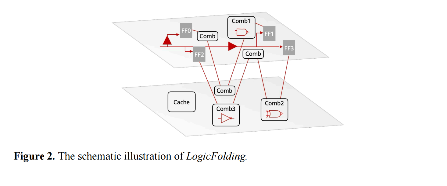
The paper adds the concept of "Gear Ratio" to describe the relationship between the Hybrid Bonding spacing and the top metal layer wiring spacing. The paper points out that only when the vertical interconnect spacing is close enough to the top metal layer spacing (the gear ratio is lower than 3, ideally close to 1), the design space can be transformed from traditional macroblock-level discrete optimization (Discrete Optimization) to unit-level continuous optimization (Continuous Optimization).
This shift is crucial, as it enables EDA tools to treat multiple active layers as a continuous whole and perform cross-layer collaborative design at standard unit granularity, instead of being limited by the extensive approach of forcibly layering by functional modules, thus unleashing the true potential of three-dimensional stacking. The paper also points out that in order to achieve this goal, Huawei has experienced many years of process development efforts in ultra-fine pitch hybrid bonding, TSV shrinkage and lamination precision control.
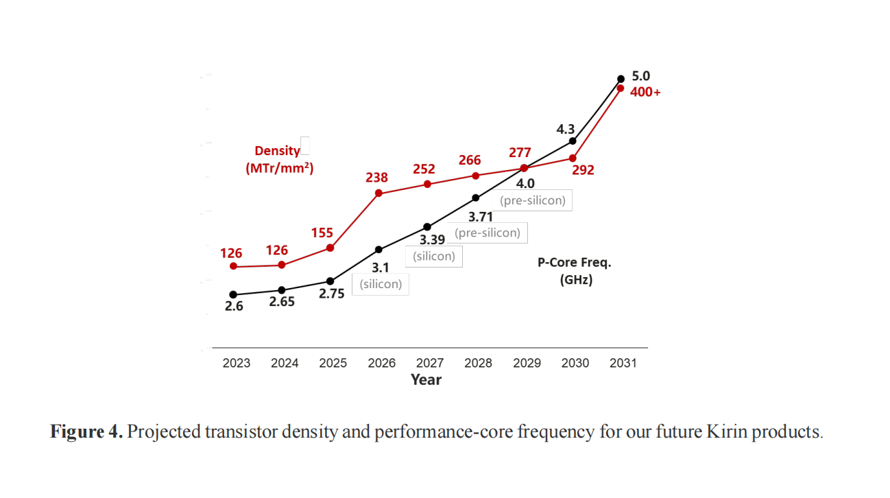
In V1, Huawei has listed the development plan for future generations of Kirin processors driven by logic folding. On this basis, V2 has added a projection curve of transistor density and CPU frequency, integrating CPU performance core frequency, transistor density, and logic folding evolution into a more complete quantitative framework. On the mobile side, V2 clearly complements the evolution path of TSV gradually moving down from the top metal layer to the M6 layer (which can release more than 30% of high-level wiring resources), and from two layers to three and four layers of multi-active layer stacking. In terms of time, Huawei Ascend 990 will introduce logical folding around 2030.
Compared with the roadmap itself, the bigger change comes from the large amount of engineering verification data added to the paper. The V2 version adds an actual measurement comparison between Kirin 2026 and Kirin9030 Pro under equal performance conditions, showing the changes in voltage, power consumption and power density of the two chips under the same performance target. The data shows that under 25°C environment and other performance targets, Kirin 2026 can reduce the supply voltage from 1.1V to 0.9V, the normalized power consumption drops to 0.59 (that is, the power consumption is reduced by 41%), and the normalized power density drops by about 5.6%.
From the perspective of the industry, while V1 mainly displays performance results, V2 supplements the engineering constraints, thermal management strategies and design methodologies behind achieving these results, further promoting the gradual evolution of τ law from a theoretical framework into a set of chip design methods that can be continuously verified.
From chip to AI cluster
In addition to mobile terminals, another noteworthy change in the V2 version is a more complete explanation of how the τ law extends from a single chip to the entire AI computing system.
Huawei believes that as large models continue to evolve, the bottleneck faced by AI systems is no longer just the computing power of a single chip, but the gradual imbalance in the development speed of multiple levels such as computing, interconnection, storage, and power supply. If AI infrastructure in the future wants to continue to improve performance, it needs to continue to compress the time constant τ from the system level, and not just rely on the evolution of a single process node.
On the specific implementation path, the updated paper further elaborates on the division of labor and collaboration of the three technologies of Unified Bus, Hi-ONE and 3D Folding in the system through multiple new schematic diagrams. The three technologies work together to optimize τ at different levels, forming a system-level collaborative design from chips, interconnections to AI clusters.
In addition, in the V1 version, Huawei also clearly proposed a series of key issues to be resolved, including an EDA tool chain adapted to three-dimensional logic division, inter-wafer process deviation compensation, vertical interconnection overhead, system energy consumption, and new benchmark testing methods. At the same time, the thermal sensing design strategy and its corresponding power density measured data are supplemented in V2.
As of press time, the paper has been clicked more than 260,000 times on the ChinaXiv platform and downloaded more than 50,000 times.
It is worth noting that Huawei did not describe τ Law as a mature solution in the two versions of the paper, but positioned it as an engineering system that continues to evolve and requires collaboration across the entire industry chain.
He Tingbo mentioned that he hopes that in the next six to ten years, enterprises, scientific research teams and industrial ecology with τ as their core research and development goals will dominate the development pattern of the computing industry in the following ten years.
"The technology development framework for the next ten years has been clear, but there are still many unsolved problems that cannot be overcome by a single company. Tool chains, industry standards, performance benchmarks, device physics, business models and other fields require collaborative creation by the entire industry." He Tingbo said.