Hybrid bonding was originally regarded as one of the most important packaging upgrades for the next generation of high-bandwidth memory (HBM), but the latest reports from Korean media show that due to the "relaxation" of industry standards, Samsung and SK Hynix are likely to suspend the adoption of this technology in the HBM4 generation and move its application node to HBM4E. JEDEC, an international organization responsible for formulating semiconductor industry standards, is re-evaluating HBM stack thickness specifications. This change not only directly affects the application timing of hybrid bonding, but also reshapes the technology game between leading storage manufacturers and large customers.
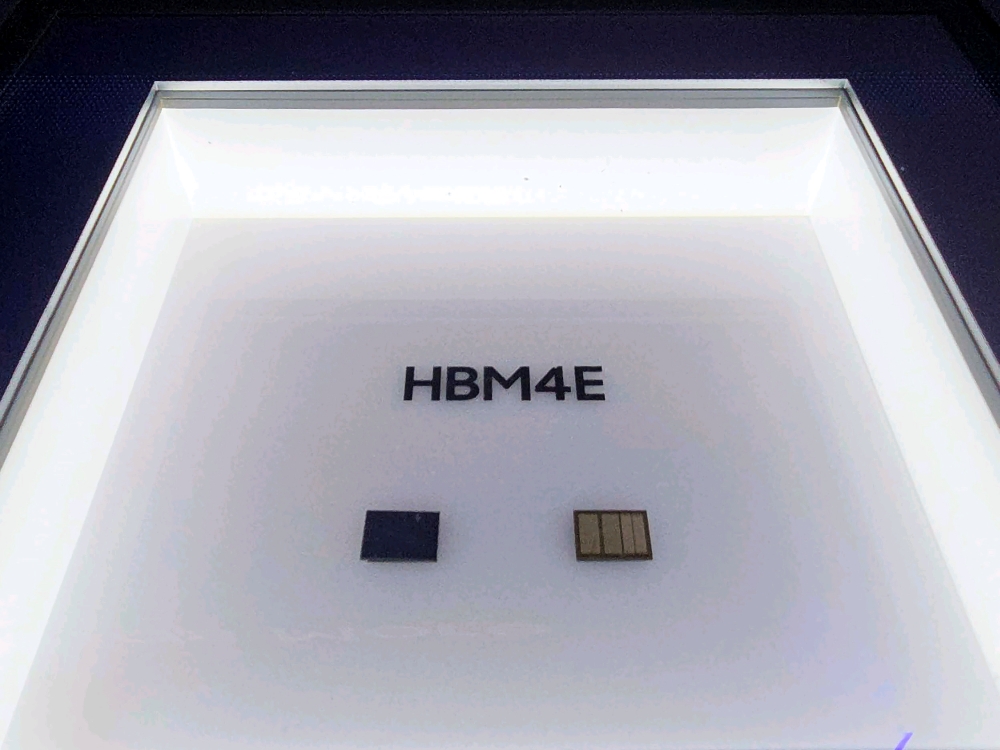
In the previous standard setting, the stacking thickness of next-generation HBM was defined as 900 microns, but the latest discussion may further relax the upper limit of thickness of HBM products to 1,000 microns. This means that chip stacking can evolve in a more "conservative" manner while maintaining acceptable mechanical and thermal design limits, without having to rely prematurely on more radical packaging routes such as hybrid bonding. For Samsung and SK Hynix, in the context that production line maturity, yield and cost still need to be balanced, such fine-tuning of standards provides more sufficient reasons to delay the adoption of new processes.
In April this year, it was revealed that SK Hynix had verified a 12-layer HBM sample using hybrid bonding. At that time, the industry expected that the company would be the first to introduce this technology in HBM4 mass production. Hybrid bonding is seen as a key layout to address the needs of next-generation AI and high-performance computing, as these applications require higher stacking layer counts and greater bandwidth density. In the traditional HBM process, each layer of DRAM chips is bonded by thermal pressure, bumps and underfill materials are arranged between the chips, and then high temperature and pressure are used to complete the stacking. Hybrid bonding improves electrical performance and heat dissipation capabilities by directly connecting metal contacts at the wafer level.
The latest report from South Korea's ZDNet states that Samsung and SK Hynix are considering temporarily "bypassing" hybrid bonding at the HBM4 stage, delaying the first node of this technology to HBM4E, while continuing to use hot compression bonding and supplemented by other heat dissipation methods on HBM4. The report reiterated previous news about JEDEC adjusting thickness standards: the stack thickness definition of HBM4 is being raised from the current 775 microns to a range of 825 to 900 microns, while the HBM5 standard may be further relaxed from 900 microns to 1,000 microns. Under this new set of parameters, manufacturers can meet design needs by increasing the stacking height or optimizing the packaging structure, without immediately moving to hybrid bonding with a higher process threshold.
What is even more noteworthy is that changes in demand from major customers are also driving this strategic adjustment. The report quoted sources as saying that "heavyweight buyers" like NVIDIA have delayed their demand for high-stack HBM, leaving internal discussions on the 16-layer HBM stack basically in a "suspended" state. Under this circumstance, HBM4E products are also likely to continue to stay in 12-layer designs, further weakening the urgency for manufacturers to adopt hybrid bonding to support higher stacking in the short term.
Despite this, Samsung and SK Hynix still hope to reap the thermal benefits brought by hybrid bonding, but intend to achieve it through alternative solutions. The report pointed out that the two companies are actively evaluating a variety of heat dissipation devices to improve the thermal conduction path under the existing thermocompression bonding structure and make up for the shortcomings of the filler material as a thermal insulation layer. In the hybrid bonding architecture, the underfill material is removed, which helps reduce temperature and improve stability. Through additional heat dissipation devices, manufacturers hope to obtain some heat dissipation dividends without changing the core bonding process.
In the long term, hybrid bonding is still regarded as a technology node that “cannot be bypassed” in the HBM field. As HBM5E continues to grow in the number of I/O ports and signal density, the report quoted industry chain sources as saying that hybrid bonding will become a "must adopt" process option during mass production of HBM5E. A higher number of input and output terminals means denser interconnections, more stringent power consumption and heat dissipation requirements, and the existing thermocompression bonding structure will face obvious bottlenecks in reliability and performance.
The current technology and standards game also reflects the delicate balance of the overall HBM market. On the one hand, the pursuit of HBM capacity and bandwidth for AI computing power and large model training continues to accelerate, forcing storage manufacturers to plan higher layers and more radical packaging technologies; on the other hand, the maturity of hybrid bonding, process yield, and packaging costs still need time to settle. "Technological leadership" alone is not enough to convince all participants to take risks. JEDEC's thickness standard adjustment provides a middle route for the industry chain to some extent, allowing all parties to have room to gradually evolve product lines within safe and controllable process boundaries.
For Samsung and SK Hynix, how to accurately divide the hybrid bonding lead-in nodes between HBM4 and HBM4E will directly affect their competitiveness in the AI storage market and their bargaining space for cooperation with major customers such as NVIDIA. If HBM4 can still meet current needs through stacking thickness and heat dissipation devices without using hybrid bonding, then concentrating on introducing new processes at the HBM4E or even HBM5E stage may become a more commercially realistic option. However, as AI application scenarios further expand and the demand for high-stack HBM re-heats, this "delayed adoption" strategy may also need to be adjusted quickly in the next few years.