
Abstract:
Changxin Technology stated in the third quarter performance exchange meeting that based on the key breakthrough of the 4F² vertical channel DRAM architecture, the sixth-generation process technology platform has completed the verification of engineering samples. This is the first time that Changxin announced that the sixth-generation process technology platform is based on the 4F² architecture.
 ,
According to industry practice, the completion of engineering sample verification means that the platform's core performance indicators have reached design expectations on real wafers, and it can enter the mass production stage after the client completes the verification. Changxin previously stated in a public speech that it is expected to launch a new generation of DDR5 RDIMM products integrating 4F² advanced technology by the end of the year for the server field, one of the most difficult fields to apply.
In terms of publicly disclosed progress, Changxin is at the forefront of the world in promoting 4F² engineering: Samsung and SK Hynix have both listed 4F² as a key direction below the 10nm level, and Changxin has taken the lead in completing engineering sample verification; if subsequent progress goes smoothly, Changxin is expected to become the first company in the world to implement 4F².
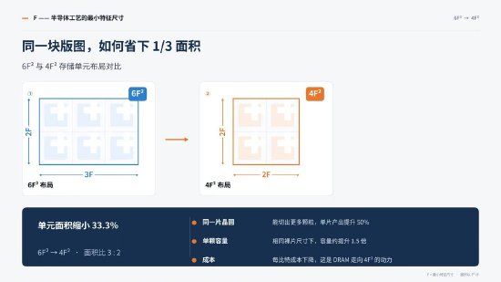
4F² is regarded as a key path to cracking the shrinkage bottleneck of DRAM cells and moving towards 3D DRAM. The evolution of DRAM technology has always revolved around density improvements - integrating more units on the same size wafer to spread the cost per bit. But after entering the 10nm level, the original 6F² has become unsustainable and is approaching the physical limit. The IEEE International Devices and Systems Roadmap (IRDS) clearly states that when half-pitch scaling becomes increasingly difficult, “the transition from 6F² to 4F² units is the most promising path to maintaining cost trends.”
The 4F² unit area is 2F×2F (F is the minimum line width or spacing achievable by photolithography technology), which is about two-thirds of the mainstream 6F² unit. It has become a common choice of major storage manufacturers around the world. SK Hynix has listed the 4F² vertical gate (VG) platform and 3D DRAM as two major technical pillars. Samsung published a 10nm 4F² paper at ISSCC 2026, and its CTO publicly confirmed in October this year that it is also developing; the industry also regards 4F² as a necessary stage to 3D DRAM.
The core of Changxin’s 4F² architecture is the self-developed VSG (Vertical Surrounding Gate) transistor. Its vertical surrounding channel structure has stronger gate control, which can alleviate short channel effects and leakage. At the architectural level, this solution decouples the manufacturing processes of DRAM and CMOS, and then realizes high-speed interconnection through wafer-level hybrid bonding, so that logic performance, storage density, and reliability can be optimized separately.
Comments