
Abstract:
The rapid expansion of the global artificial intelligence industry is causing serious shortages in the supply of memory chips, especially the surge in demand for high-bandwidth memory (HBM), which has put traditional DRAM production capacity under pressure to reallocate. In this context, former Intel CEO Pat Gelsinger is betting on a new type of memory technology, hoping to solve the long-term capacity, bandwidth and power consumption problems faced by AI chips by changing the way traditional memory cells are designed.
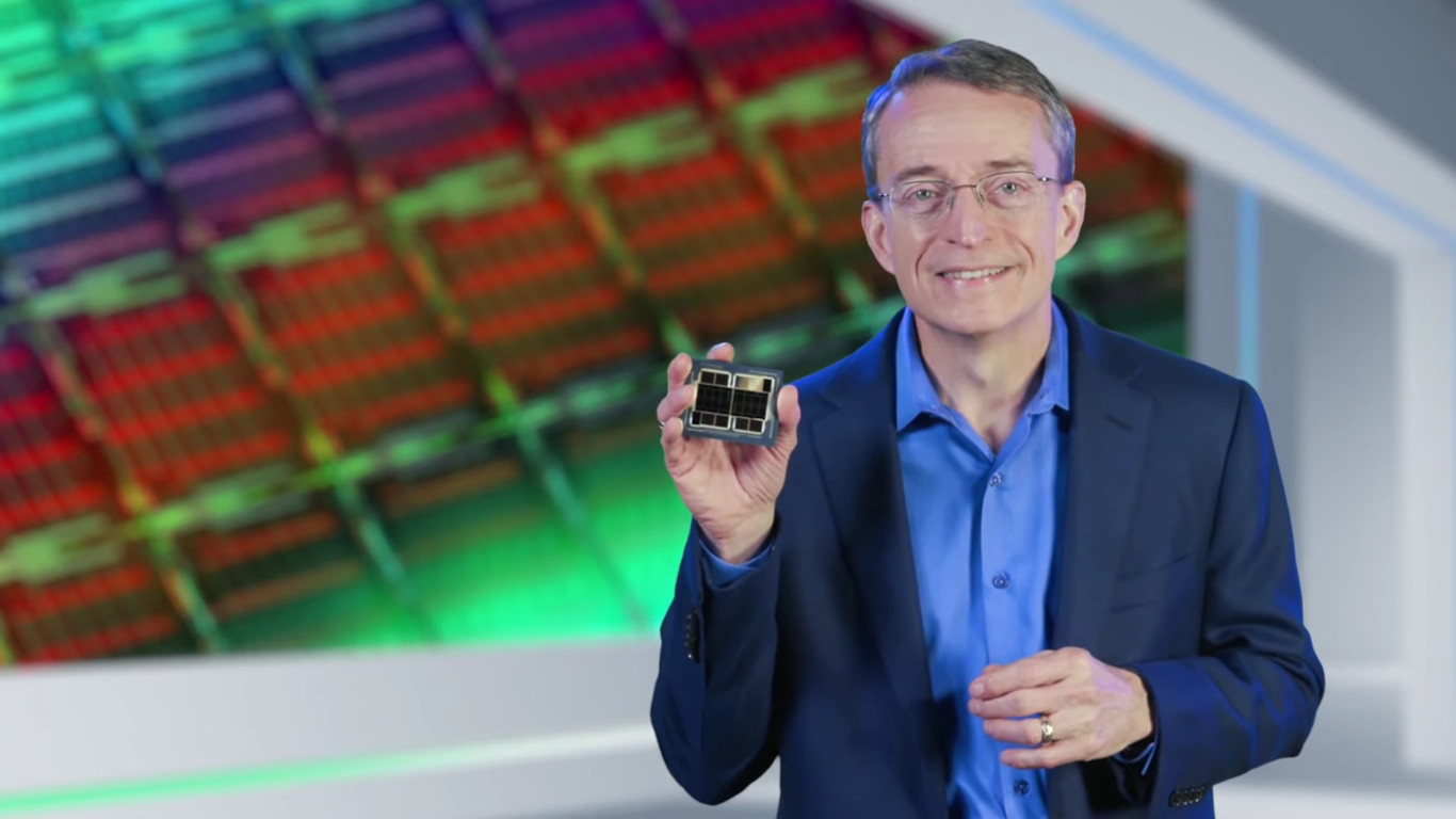
The technology is called Z2RAM and was developed by US start-up Nagare Labs. The company was founded by Georgia Institute of Technology researchers Suman Datta and Shimeng Yu. Its research foundation comes from years of exploration of new storage technologies such as ferroelectric memory and resistive random access memory.
Playground Global, the investment institution Kissinger is currently involved in, led Nagare Labs’ $5 million seed round of financing. He has shown considerable interest in this technology and believes that Z2RAM has the opportunity to combine the advantages of SRAM, DRAM and flash memory to create a new type of memory with high density, high speed and scalability.
Kissinger pointed out that in the past three decades, mainstream storage technologies that have been widely commercialized have not undergone fundamental changes. SRAM, DRAM and NAND flash memory still form the storage foundation of modern computing equipment. However, as the computing requirements of artificial intelligence grow rapidly, the limitations of traditional storage architectures are becoming increasingly obvious.
The most important breakthrough of this technology is to redesign the way the memory cell stores charge.
Traditional DRAM usually uses a 1T1C structure, that is, a transistor is paired with a capacitor, and the capacitor stores charge to represent data. Because the charge in the capacitor leaks out over time, DRAM must refresh data periodically, and the read process is destructive and requires rewriting after reading.
SRAM uses a different design, usually requiring six transistors to form a memory cell. It does not need to be refreshed periodically like DRAM, and the read speed is very fast, so it is widely used as a cache inside the processor. However, the price is that the storage unit area is larger and the manufacturing cost is high, making it difficult to achieve large-scale and high-density expansion like DRAM and NAND.
Z2RAM tries to find a new balance between the two. It uses two transistors to form a memory unit, instead of using a separate capacitor in traditional DRAM. Instead, it uses the gate capacitance of the second transistor to store charge.
Suman Datta, co-founder of Nagare Labs, explained that this design enables non-destructive reading. In other words, when reading data, there is no need to consume the storage charge and then perform a rewrite operation like traditional DRAM, so it is expected to reduce access latency and improve overall storage efficiency.
In terms of density, Nagare Labs predicts that the storage density per unit area of the first-generation Z2RAM can be more than five times that of traditional SRAM. For example, if SRAM of the same area can provide 64MB capacity, then using Z2RAM, the capacity can theoretically be increased to about 320MB while maintaining a bandwidth level close to that of SRAM.
This is especially important for artificial intelligence processors. Currently, AI accelerators increasingly rely on HBM to provide huge memory bandwidth, but HBM requires complex stacking packaging technology, high manufacturing costs, and limitations in power consumption and packaging area.
On the other hand, some processors specifically used for AI inference use a large amount of on-chip SRAM to minimize the delay of the processor accessing external memory. However, the density of SRAM is limited, causing the chip to make a trade-off between capacity and computing units within a limited area.
For example, NVIDIA Groq 3 LPU uses a large amount of SRAM as on-chip storage resources, and the SRAM capacity of a single chip is approximately 500MB. According to Nagare Labs’ technical vision, if Z2RAM can achieve the expected five times density, then the same area can accommodate several times the data of traditional SRAM. This may reduce the number of processors required for large AI inference systems and reduce the pressure on data to be transferred between different chips.
Another important feature of Z2RAM is the use of oxide semiconductor materials, which are planned to be directly integrated on top of the computing logic chip through 3D hybrid bonding technology.
This means that it does not have to rely entirely on the traditional architecture of separating the memory chip from the processor. Instead, it has the opportunity to stack high-density storage layers directly near the computing chip to shorten the data transmission distance. Its design idea is somewhat similar to AMD's stacking of additional SRAM cache on the processor through 3D V-Cache technology, but Z2RAM hopes to provide higher storage density.
In terms of manufacturing technology, Nagare Labs also plans to draw on the vertical stacking idea of NAND flash memory to build multiple storage layers layer by layer. Unlike HBM and LPDDR, which rely on complex high-density memory packaging, the company hopes to achieve relatively simple multi-layer manufacturing through oxide semiconductors and back-end processes. If this solution is successful, it will have the opportunity to reduce the manufacturing cost of large-capacity on-chip storage.
However, Z2RAM is still in a very early stage of development. Nagare Labs has just completed a US$5 million seed round of financing. The results at this stage are mainly laboratory prototypes and have not yet entered the mature chip manufacturing stage.
The company is looking for fab partners who can provide R&D and manufacturing capabilities, hoping to advance the technology from the clean room environment of a university laboratory to larger-scale production verification. According to the current plan, Nagare Labs hopes to provide working Z2RAM memory chip samples within the next four years and strive to achieve commercial shipments within the next ten years.
At the same time, this technology also faces many engineering challenges.
The first is the integration issue with computing chips. Z2RAM needs to be connected to the processor or AI accelerator through 3D hybrid bonding, but the industry has not yet formed a unified interface standard suitable for this new type of memory. Georgia Tech researchers said that without mature industry standards, Nagare Labs may need to develop its own interface technology, which will increase the complexity of product design and commercialization.
The second is material reliability. Oxide semiconductors have certain advantages in thermal stability and radiation resistance, but defects such as atomic vacancies may occur within the material. These microscopic defects can affect the threshold voltage of the transistor, and even small voltage changes can cause data errors in the memory cell.
For memory products, reliability is often more important than peak performance in the lab. Any new storage technology must undergo long-term data retention, read and write life, temperature changes and manufacturing consistency verification before it can truly enter the commercial market.
The co-founder of Nagare Labs also admitted that there have been a large number of memory startups in history that have tried to challenge traditional DRAM and flash memory technology, but ultimately failed. Even if a technology performs well in the lab, that doesn't mean it will pass the semiconductor industry's stringent quality standards and enter the supply chain for existing computing systems.
The reason why Kissinger is optimistic about Z2RAM is closely related to the memory bottleneck faced by the current AI industry. The training and inference of large language models not only require powerful computing power, but also require continuous feeding of large amounts of data to the processor. When the processing speed of the computing unit far exceeds the data supply capacity of the memory, the processor must wait for data, resulting in expensive computing resources that cannot be fully utilized.
Currently, HBM is the main solution to solve the memory bandwidth problem of AI accelerators, but it is not without flaws. Gelsinger believes that if Z2RAM can achieve expected performance, it will have the opportunity to provide solutions different from existing HBM in terms of storage density, speed and power consumption.
It is worth noting that Z2RAM is not a technology that can solve the global DRAM and HBM supply shortage in the short term. Even if engineering samples become available in the next four years, large-scale commercialization is still a long way off. The current tight supply of global memory is mainly caused by the surge in demand from AI data centers, and Samsung, SK Hynix and Micron shifting more production capacity to HBM and server memory products.
Ars Technica
+2
If Z2RAM can eventually achieve mass production, its more important significance may lie in changing the storage architecture of future processors, rather than simply increasing the supply of traditional memory chips. It is expected to allow AI processors to obtain larger high-speed storage space inside the chip, reduce dependence on external memory bandwidth, and provide new design options for the next generation of AI accelerators.
From SRAM to DRAM to NAND flash memory, the semiconductor industry has formed a relatively mature storage technology system. Z2RAM attempts to break the long-standing performance versus density trade-off between these technologies. However, it is still a technical concept in the laboratory stage. Whether it can eventually be transformed from a scientific research result into a competitive commercial product will require time and manufacturing process testing.
Comments