
Abstract:
The next capacity competition for AI computing power is extending from GPUs to silicon photonic chips. Wafer foundry Tower Semiconductor is aggressively expanding its silicon photonics production capacity in Japan. Tower CEO Russell Ellwanger recently stated that AI data centers are driving the rapid growth in demand for silicon photonic chips and the company needs to expand production capacity as soon as possible. Japan will become one of Tower's most important optical communication semiconductor production bases in the world.
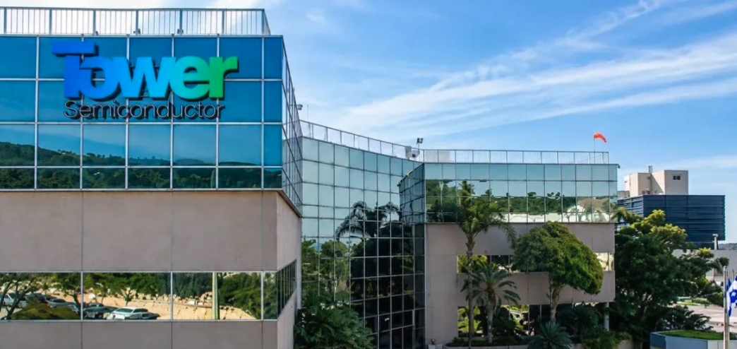
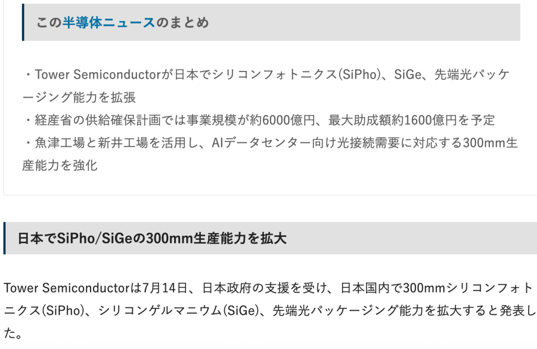
According to Tower's previously announced plan, the company will invest more than 600 billion yen, or approximately US$4 billion, in Japan, focusing on expanding its 300mm silicon photonics, silicon germanium and advanced optical packaging capabilities. Among them, the Japanese government plans to provide up to approximately 160 billion yen and approximately US$1 billion in support.
For Tower, this is not only an ordinary round of fab expansion, but also a long-term bet in the era of AI data centers, 800G/1.6T optical modules, NPO and CPO.
1. AI pushes silicon photonics into a production expansion cycle
Why does Tower have to expand production now?
There is only one core reason: more and more data needs to be transmitted between AI servers.
When the AI cluster expands from thousands of GPUs to tens of thousands or even hundreds of thousands of GPUs, what really limits the scale of computing power is no longer just the GPU itself, but also how to exchange data at high speed between GPUs. Traditional copper interconnects are facing increasing pressure in terms of distance, bandwidth, signal integrity and power consumption, and optical interconnects are therefore beginning to move closer to servers and chips.
The value of silicon photonics technology is to use mature silicon processes to manufacture photonic devices such as modulators, photodetectors, and waveguides, and work together with electronic chips to allow more high-speed data to be transmitted through optical signals.
This is why after 800G, 1.6T optical modules, silicon photonics, NPO and CPO are becoming the core keywords of the AI data center industry chain.
Tower CEO Ellwanger said that the current market demand for silicon photonic chips is very high and the company must increase production capacity as soon as possible.

△Tower Semiconductor CEO Russell Ellwanger
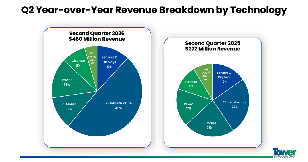
The information disclosed by Tower shows that its silicon photonics business has entered a stage of rapid growth. The company is not only locking in future orders, but also beginning to plan production capacity in 2027 and even 2028 in advance.
In other words, what Tower is now competing for is not today’s optical module orders, but the manufacturing entrance to AI optical interconnection infrastructure in the next few years.
2. Why is Tower betting on silicon light?
Tower is different from TSMC, Samsung, and Intel. It does not focus on the most advanced CPU and GPU logic processes as its main battlefield, but has long-term focus on specialty process wafer foundry.
Tower's technology landscape covers silicon photonics, silicon germanium SiGe, radio frequency RF, power management, image sensors and other fields. In the AI era, this does not seem to be pursuing the "2nm, 1.4nm" route, but has gained new growth opportunities.
In addition to GPUs, AI servers also require a large number of high-speed network chips, optical modules, optoelectronic chips and high-speed analog devices.
Especially in the field of silicon photonics, Tower has formed a deep process accumulation.
Tower's PH18DA and other platforms are aimed at high-speed optical communication applications and can integrate lasers, optical amplifiers, modulators, photodetectors and other devices, providing a manufacturing basis for 800G, 1.6T and next-generation high-speed optical interconnections.
This makes Tower a very special role in the AI optical communications industry chain: it does not produce GPUs, but it may manufacture key silicon photonic chips needed to connect a large number of GPUs.
3. US$4 billion bet on Japan
The scale of Tower's Japanese production expansion plan exceeds 600 billion yen, which is approximately US$4 billion, and is mainly promoted along two routes.
The first route is to use Tower to rapidly expand silicon photonics production capacity in existing wafer fabs in Japan.
Tower plans to transform its Arai factory in Myoko City, Niigata Prefecture, and use related manufacturing resources for 300mm silicon photonics and advanced optics-related production; at the same time, the company will further increase the 300mm wafer manufacturing capacity of Uozu Fab 7 in Toyama Prefecture.
Fab 7 currently has a manufacturing foundation related to silicon germanium and silicon photonics. Therefore, Tower can complete equipment introduction, process verification and mass production ramp-up faster than building a new wafer factory from scratch.
Tower predicts that this new capacity will reach mass production readiness in the fourth quarter of 2027.
The second route is more radical.
Tower plans to continue to build new 300mm manufacturing facilities near Fab 7 to further expand silicon photonics and silicon germanium production capacity. The new production capacity is expected to make a substantial contribution to the company's revenue starting around 2029.
According to Tower's plan, after the completion of relevant projects, its equivalent Japanese 300mm wafer production capacity is expected to reach approximately 45,000 wafers per month.
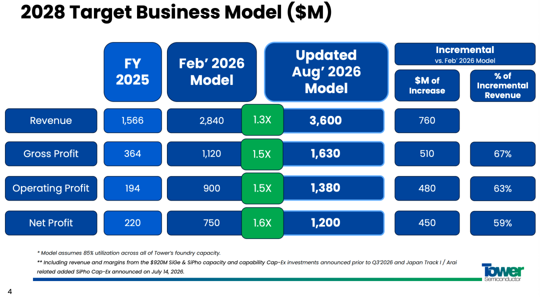
This means that Japan will become one of the most important manufacturing bases for Tower's next round of silicon photonics expansion. (As shown in the picture - 2028)
4. Why did Japan give Tower $1 billion?
Behind Tower's large-scale investment in Japan is the Japanese government's strategy to promote the reconstruction of the semiconductor supply chain.
Japan’s Ministry of Economy, Trade and Industry plans to provide support of up to approximately 160 billion yen, or approximately US$1 billion, to the Tower project, focusing on supporting next-generation communication semiconductor manufacturing capabilities such as silicon photonics and silicon germanium.
The Japanese government has supported TSMC’s Kumamoto factory, the Rapidus advanced logic project, and a number of semiconductor materials, equipment and packaging projects in recent years. The silicon photonics manufacturing capabilities represented by Tower have complemented the AI high-speed optical interconnection.
According to relevant arrangements, Tower needs to assume long-term production and supply responsibilities. In the event of tight semiconductor supply, the Japanese market will also receive corresponding supply guarantees.
Therefore, this subsidy is not just about “inviting Tower to build a factory in Japan.”
What Japan really hopes to obtain is a key manufacturing node that can serve the future AI data center, optical communications and optoelectronic integration industries.
5. Tower Japan’s layout also has another advantage: the people left behind by Panasonic
Tower chose Japan for another reason that is often overlooked—talent.
Tower entered Japan as early as 2014 by establishing TPSCo with Panasonic and took over Panasonic's semiconductor manufacturing resources in the Hokuriku region.
Although Panasonic later gradually exited part of its semiconductor manufacturing business, a large number of engineers, craftsmen and industrial foundations with wafer manufacturing experience were retained.
For semiconductor manufacturing, this is very important.
A fab cannot produce just by buying equipment. Process integration, equipment maintenance, yield improvement, defect control and mass production experience require long-term accumulation.
Therefore, Tower can directly use existing factories, infrastructure, engineering teams and supply chain systems to expand production in Japan, rather than building a new manufacturing base from scratch.
This is also an important reason why Tower chooses to continue to focus heavily on Japan.
6. The real next battle: CPO
However, the competition Tower faces is also escalating.
In the past, silicon photonic chips were mostly used in pluggable optical modules, but as the bandwidth of AI switching chips continues to increase, optical devices are getting closer and closer to switching ASICs and computing chips.
So the industry began to move from traditional pluggable optical modules to NPO, and then further to CPO.
CPO, Co-Packaged Optics, co-packaged optics.
The core idea is to move the optical engine closer to the switching chip and reduce power consumption and signal loss by shortening the transmission distance of high-speed electrical signals.
This means that the future silicon photonics competition will not only be "who can produce silicon photonic chips", but also include who can integrate silicon photonics, advanced packaging, switching ASICs, chiplets and high-speed interconnects into a system.
Wafer foundry companies such as TSMC, Tower, and GlobalFoundries are all planning in this direction.
For Tower, one of the important tasks of Japan's production expansion is to prepare manufacturing capabilities in advance for the next stage of CPO competition.
7. Tower may form synergy with Japan’s NTT
Japan also has an important silicon photonics card - NTT.
NTT Group ≈ A mixture of China Telecom + China Mobile + China Information Technology + large IT service providers (similar to Digital China/Huawei government and enterprise).
If you only look at fixed network + optical fiber base, it is closest to
China Telecom
; Its mobile subsidiary NTT DOCOMO≈China Mobile
; NTT DATA is a top IT integrator.NTT has been promoting the IOWN (Innovative Optical and Wireless Network) plan for a long time, hoping to use photoelectric integration technology to reduce energy consumption in data centers and communication networks.
One of the important directions is to keep "light" moving into the computing system.
From optical connections between data centers, to servers, to optical interconnections at the board level and even near chips, optoelectronic integration is becoming an important technical route for Japan's next-generation communications industry.
Companies such as NTT Innovative Devices, Shin Kong Electric, Broadcom and Accton have already cooperated on optical engines, substrates, switching ASICs and system integration.
Tower happens to be able to provide one of the key links: silicon photonics and silicon germanium wafer manufacturing.
If the two sides further deepen cooperation in the future, Japan may gradually form:
Silicon photonic wafer manufacturing → Optical engine → Advanced substrate → CPO/NPO → Switch → AI data center
Such a more complete industrial chain.
Ellwanger said that there is a possibility when talking about potential cooperation with NTT, but specific cooperation details have not been announced yet.
8. Japan is competing for the "optical chip era"
Japan once lagged far behind TSMC and Samsung in the field of advanced logic manufacturing, but the AI era has given Japan a window to reorganize the semiconductor industry.
This window is not necessarily just 2nm.
Silicon photonics, silicon germanium, advanced packaging, optoelectronic integration, CPO, and high-speed optical modules are also likely to become important growth directions for the semiconductor industry in the next decade.
Tower invested US$4 billion to expand production in Japan, so it is worth understanding in a larger industrial context.
On the one hand, Tower needs a large amount of silicon photonics production capacity to meet the needs of AI data centers; on the other hand, Japan hopes to re-establish key semiconductor manufacturing capabilities. Tower needs Japan’s engineers, manufacturing foundation and policy support, while Japan needs Tower’s silicon photonics technology and global customers.
The interests of both parties converge at this point in time of AI optical interconnection.
As GPUs become faster and AI clusters become larger, how data moves between hundreds of thousands of chips will become a new bottleneck.
One of the most important questions in the semiconductor industry over the past two decades has been: Who can make the most advanced transistors?
In the next ten years, another issue may become increasingly important:
Who can connect hundreds of thousands of AI chips with faster and lower power consumption light?
Tower is betting $4 billion on the answer.
Comments