
Abstract:
As TSMC accelerates the development of next-generation advanced processes, the possible location of its future 1-nanometer chip production base has unexpectedly attracted attention from the outside world. Wu Chengwen, political affairs member of Taiwan's Executive Yuan and chairman of the National Science and Technology Commission, gave a speech at the IEEE Asia Solid-State Circuits Conference, which was regarded by the industry as revealing the development direction of TSMC's future 1-nanometer manufacturing base in advance.
When talking about the future development plan of Taiwan's semiconductor industry during the meeting, Wu Chengwen said that the authorities plan to build a new park within the Tainan Science Park system to support the development and production of 1-nanometer process technology. He emphasized that as the 2-nanometer process enters the mass production stage, the more advanced 1-nanometer technology not only requires breakthroughs at the process level, but also requires the cooperation of land, water resources, and a complete supply chain system.
Although Wu Chengwen did not directly mention the name of TSMC, because currently the only company in Taiwan with the most advanced logic chip manufacturing capabilities is TSMC, it is generally believed that the relevant planning will almost certainly revolve around TSMC.
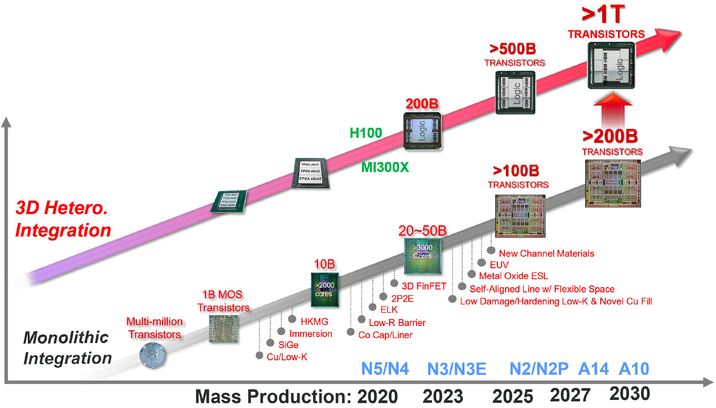
According to the speech, the development of the new park is expected to start in 2027. This means that while promoting 2nm mass production and 1.4nm (A14) node construction, TSMC may have begun infrastructure layout for the longer-term 1nm process.
Currently, TSMC has officially confirmed that the A14 process, which is a 1.4-nanometer process technology, is scheduled to be put into mass production in 2028. At the same time, news from the supply chain shows that TSMC may advance the relevant timetable and start risk trial production as soon as the second half of 2027. There are even rumors that some mass production preparations may be advanced to around October 2027.
Risk trial production is an important stage of chip manufacturing. Before entering full-scale mass production, the fab will use this stage to verify equipment operation, test process stability, and eliminate potential problems to prepare for subsequent mass production.
In fact, TSMC is currently actively expanding its A14 process capacity layout. Previously public information showed that the company is promoting the construction of multiple 1.4nm wafer fabs in the Central Taiwan Science Park and plans to start mass production in 2028. The A14 process is regarded as TSMC's key technology platform for promoting the development of artificial intelligence, high-performance computing and advanced data centers in the future.
In addition to discussing advanced semiconductor manufacturing, Wu Chengwen also focused on future key industries such as robotics and optical communications in his speech. He said that the development of the robot industry will create opportunities for metal processing, plastic materials and related manufacturing companies to enter high value-added industrial chains, thus enhancing the overall industrial competitiveness.
In the field of optical communications, he pointed out that the development of related technologies should not be limited to the connection between server racks in data centers, but should be expanded to more application scenarios. As the demand for artificial intelligence computing power continues to grow, high-speed optical communication is regarded as an important infrastructure to support large-scale data transmission in the future.
In recent years, with the rapid development of the global artificial intelligence industry, the demand for advanced process chips has continued to rise. As the world's largest foundry, TSMC has become a core beneficiary of this trend. From 2 nanometer to 1.4 nanometer, and then to the future 1 nanometer node, the company is continuing to increase R&D and capital investment to maintain its leading position in the global advanced process field.
Although TSMC has not officially announced the specific location of its 1-nanometer production base, judging from information released by Taiwan’s science and technology authorities, the Tainan Science Park system is becoming an important candidate area most likely to host the next generation of ultra-advanced processes. If the relevant plans are finally implemented, Tainan is also expected to further consolidate its position as a global advanced semiconductor manufacturing center.
Comments