
Abstract:
As the world's largest and most advanced semiconductor manufacturer, TSMC's progress in SRAM shrinkage has been stagnant for many years. Since the mass production of the N5 5nm process in 2020, the area of 6T SRAM memory cells has remained at about 0.021 square microns. The transistor density of logic components continues to increase, but memory has not kept up with the same pace. With the arrival of the A14 node, which is scheduled to be put into production in 2028, this situation is expected to be broken:
TSMC’s 6T SRAM memory unit is expected to shrink to 0.017 square microns, a decrease of approximately 19%. This means that TSMC has made a breakthrough in related technologies and is preparing to push it into mass production with the help of the A14 node.

TSMC is currently conducting trial production to evaluate the feasibility of this node, while allowing customers to test the actual performance of their designs in TSMC's production environment. The progress of the A14 node is quite optimistic. Due to the smooth early progress, the schedule has been advanced. If trial production continues smoothly and no major yield or production problems occur, risk trial production will start in 2027, followed by mass production in 2028. If there are no obvious obstacles next year, TSMC may even advance the mass production schedule by a few months.
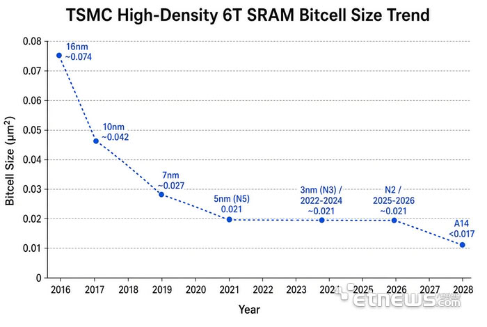
Compared with the recently announced mass production of the N2 2nm node, the A14 process can provide up to 15% speed improvement at the same power consumption, or achieve up to 30% power consumption reduction at the same frequency. TSMC also claims that the logic density has increased by 20% and the SRAM density has increased by 19%. This progress is significant: Logic circuits and memories can now be scaled effectively over much larger generation spans, in stark contrast to the sub-10nm era. The A14 node will be first introduced at TSMC’s headquarters factory in Taiwan, where the company plans to start mass production in 2028.
Comments