
Abstract:
With the global demand for artificial intelligence computing power continuing to explode, TSMC is advancing the layout of advanced processes at an unprecedented speed. The latest industry news shows that TSMC's 1.4nm A14 process development is progressing smoothly, and trial production is expected to start in the first quarter of 2027 at the earliest. At the same time, driven by strong demand for AI chips, the company's 3-nanometer process production capacity is rapidly expanding, and it is expected that the monthly production capacity will exceed 200,000 wafers by the end of 2027.
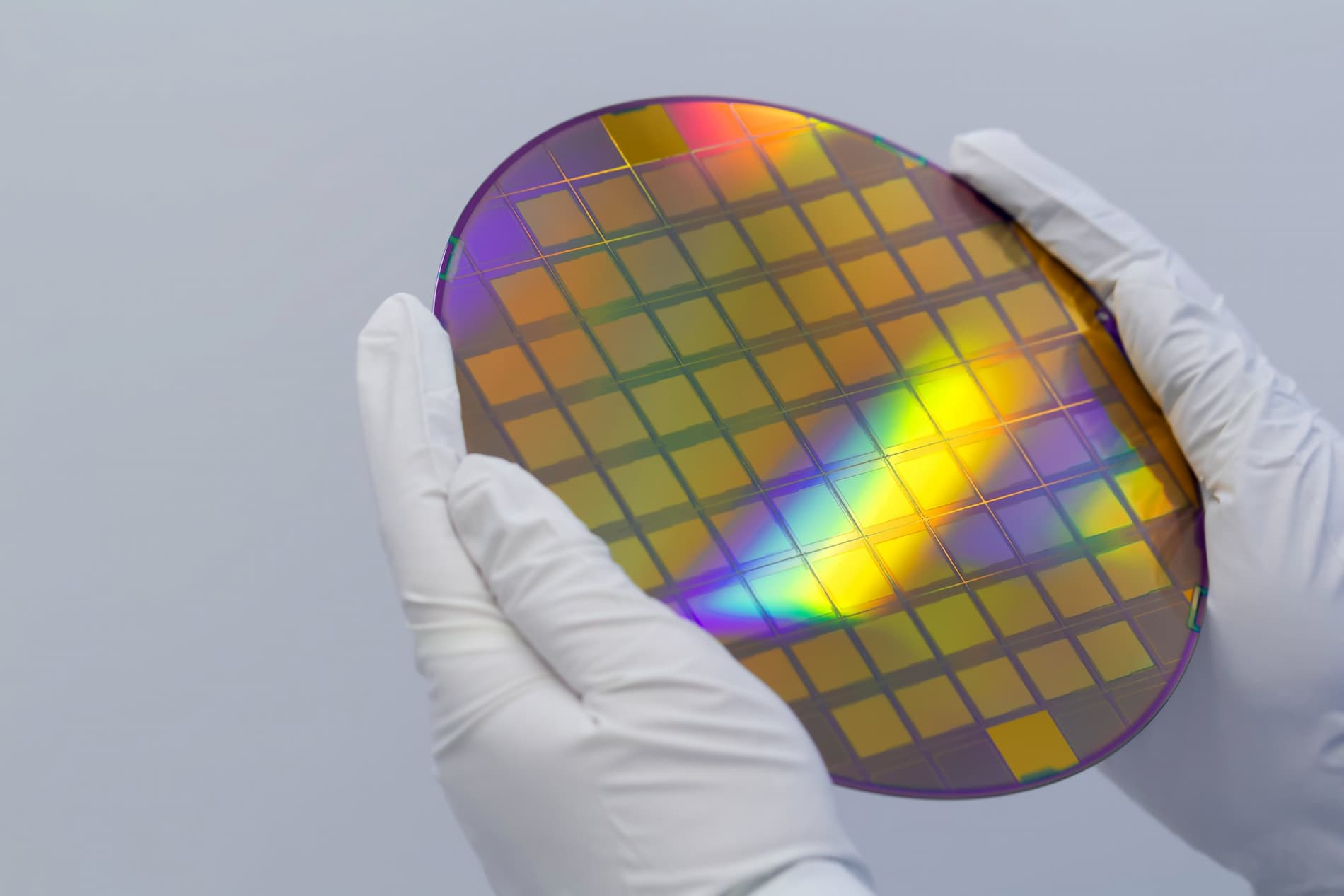
According to the latest information disclosed by the industry chain, TSMC is accelerating the advancement of the A14 process. A14 is TSMC's important angstrom-level manufacturing node after 2 nanometers. It is also an important basic process for future artificial intelligence, high-performance computing and next-generation mobile processors.
Currently, TSMC has planned multiple advanced wafer fabs in Taiwan specifically for the A14 process. News shows that some of these factories can start trial production as early as the first quarter of 2027. However, the main production base in Taichung is expected to complete the main construction in the second quarter of 2027, so the plant's large-scale trial production is expected to fall around the third quarter of 2027.
The industry generally believes that core customers such as Apple have locked in relevant production capacity in advance. Market news points out that Apple’s future A22 Pro processor is expected to be one of the first important products to adopt the A14 process and is expected to officially enter the market in 2028.
In addition to 1.4nm, TSMC’s most important current growth driver still comes from the artificial intelligence industry’s strong demand for the 3nm process.
As NVIDIA, AMD, Broadcom and many AI accelerator manufacturers continue to expand the scale of orders, TSMC's 3-nanometer production line continues to set production records. Data shows that the monthly production capacity of the 3-nanometer production line in the Southern Science Park is expected to reach 170,000 to 180,000 wafers in the fourth quarter of 2026, and by the end of 2027, this number is expected to exceed 200,000 wafers.
Industry analysts believe that demand for AI chips has become the most important factor driving the expansion of advanced processes. Whether it is large-scale language model training, inference servers, or enterprise-level AI infrastructure construction, a large amount of advanced manufacturing capacity is being consumed. In order to meet market demand, TSMC not only continues to build new factories, but is also converting some existing process equipment to 3nm production to improve overall supply capabilities.
At the same time, TSMC’s 2-nanometer process is also rapidly expanding output. The market predicts that by the end of this year, the monthly 2-nanometer production capacity is expected to reach 90,000 to 100,000 wafers, further consolidating its leading position in the advanced process field.
In contrast, although Samsung Electronics has also formulated a 1.4nm development plan, its current public roadmap shows that the commercialization time of its related processes is expected to be around 2029. Judging from the current progress, TSMC still maintains a clear lead.
Analysts pointed out that the competition for advanced manufacturing processes is no longer just a technical competition in the field of mobile phone processors, but has become a battle for basic computing resources in the era of artificial intelligence. Whoever can take the lead in providing advanced processes with stable, high yield and large-scale mass production will have the say in the future AI chip industry chain.
In an environment where the demand for artificial intelligence continues to grow, TSMC is further consolidating its position as the world's leading foundry by simultaneously promoting 2 nanometer, 1.4 nanometer and large-scale expansion of 3 nanometer production lines. As the A14 process gradually approaches the trial production stage, the next round of advanced semiconductor competition has begun in advance.
Comments