
Abstract:
A team from the University at Buffalo used first-principles calculations to predict what kind of optical "fingerprints" different atomic defects in hexagonal boron nitride would produce when encountering laser light. The study analyzed ten types of defects, including boron or nitrogen atom vacancies, and defect structures formed by carbon atoms replacing boron and nitrogen positions, and found that they would change the intensity and polarization characteristics of the light signal generated by the material.
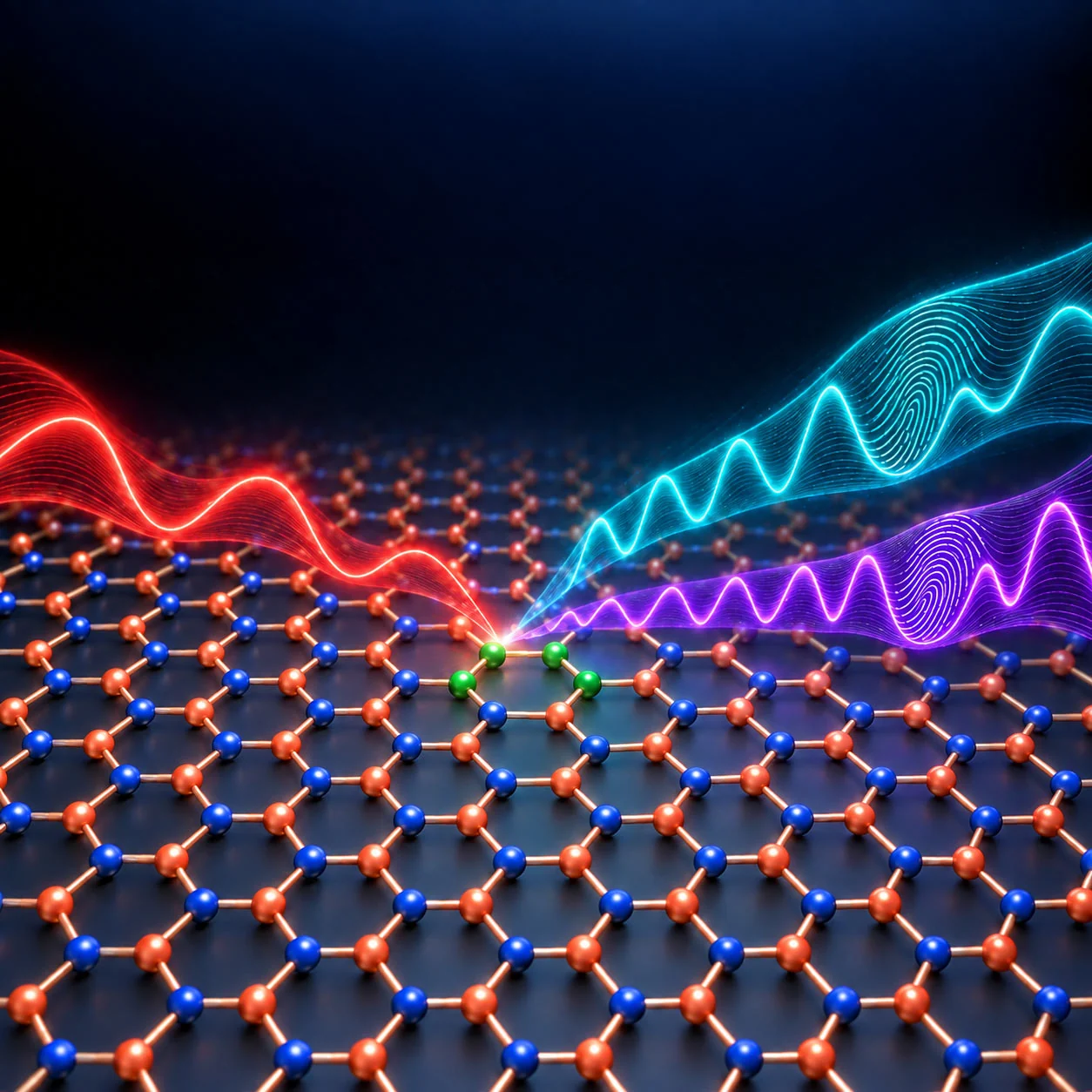
Hexagonal boron nitride is a two-dimensional material that has attracted attention, consisting of boron and nitrogen atoms arranged in a honeycomb structure. Research shows that defects have little impact on the material's ordinary linear optical response, but can significantly enhance the nonlinear optical effect: some structures can allow the incident laser to generate light with twice or triple the frequency. Among them, the second harmonic signal of the carbon atom defect complex can be enhanced by several orders of magnitude, and the signal changes with the polarization direction.
These differences are expected to help researchers tell which atoms the defects contain and how they are arranged. Even if the defect consists of the same kind and number of atoms, the resulting polarization spectrum may be different as long as the geometry is different. For example, of two four-carbon arrangements simulated by the study, one was expected to produce a strong signal in both polarization directions, while the other was significantly enhanced in only one direction. The research team also measured carbon-doped boron nitride samples, and the experimental results qualitatively supported the trends predicted by the calculations; however, this work has not yet demonstrated a mature detection device that can identify single atomic defects one by one.
Some hexagonal boron nitride defects can emit one photon at a time and are expected to be used in quantum communications and high-sensitivity sensing. Researchers hope to use these optical characteristics to screen out defects suitable for generating quantum light and further control their location in the material, ultimately creating an array composed of multiple precisely arranged quantum light sources. Relevant research was published in Nano Letters. Currently, it mainly provides theoretical basis for identifying and designing defects. Practical quantum devices still require subsequent verification and engineering development.
Comments