
Abstract:
Elon Musk’s Terafab semiconductor manufacturing project is further expanding its planning scale. According to a Wccftech report on November 8, Terafab, the semiconductor joint venture formed by Tesla and SpaceX, has revealed to semiconductor equipment suppliers that it plans to achieve a monthly production capacity of 1 million wafers by 2032. Among them, memory chips will account for the vast majority, with a target of 700,000 pieces per month, and the other 300,000 pieces will be used to produce logic chips.
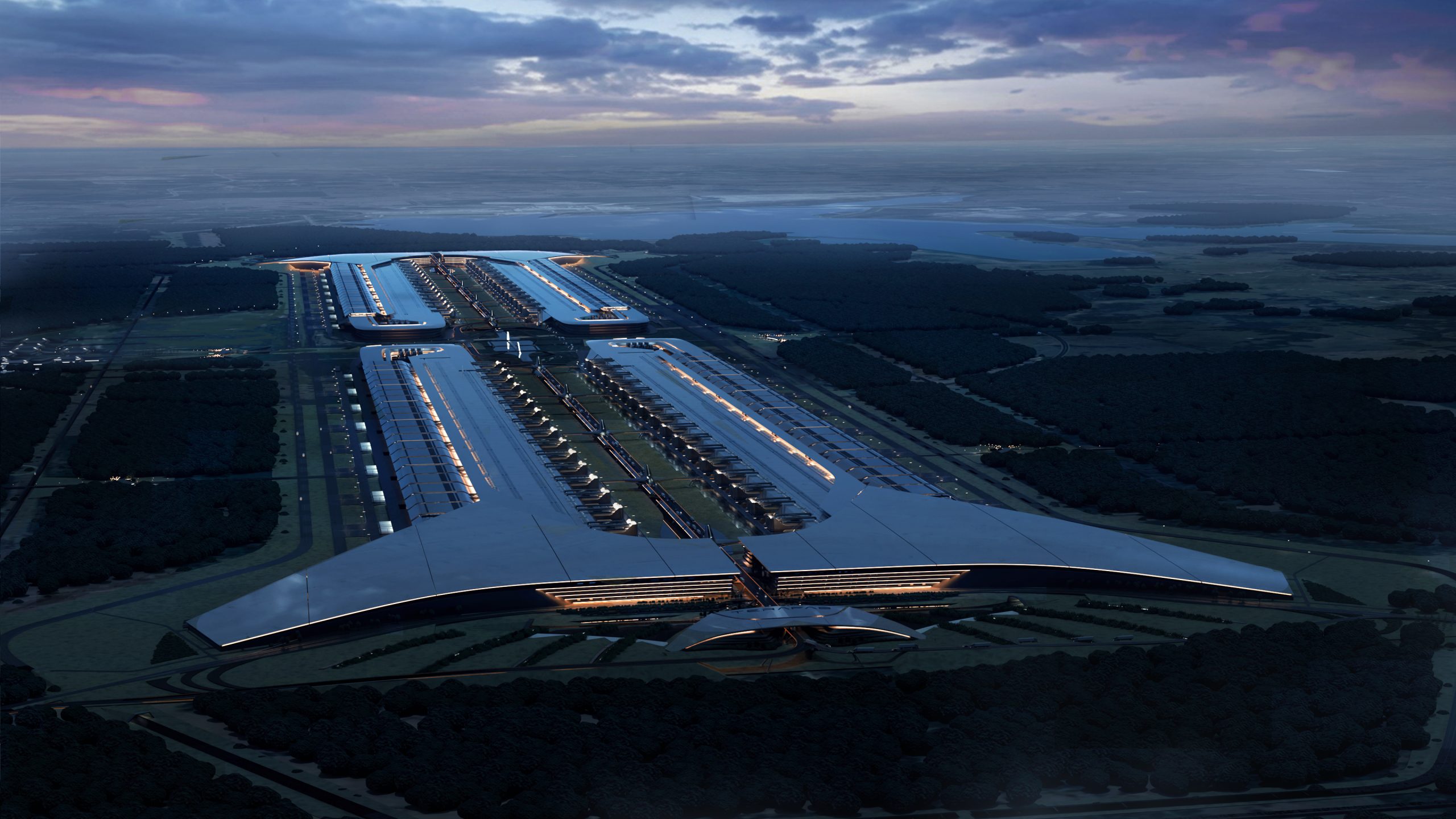
If this goal is ultimately achieved, Terafab's memory chip production scale will reach the level of Samsung's current DRAM wafer production capacity. According to data cited in the report, Samsung’s current monthly DRAM wafer production capacity is approximately 650,000 to 700,000 pieces. For an emerging semiconductor manufacturing company that is still in the early stages of construction and has no mature mass production experience, this is undoubtedly an extremely aggressive expansion plan.
Terafab is an important project for Musk to promote the vertical integration of the semiconductor industry. It is jointly participated by Tesla and SpaceX and receives technical support from Intel. Its core goal is to get rid of its high dependence on external chip suppliers and provide a stable and sufficient supply of computing chips and memory for Tesla's humanoid robot Optimus, autonomous driving systems, and SpaceX's future space data centers.
Musk previously proposed that Terafab ultimately hopes to achieve 1,000 gigawatts, or 1 terawatt, of AI computing power per year. This goal goes far beyond the positioning of a traditional semiconductor factory and is closer to a comprehensive industrial system covering chip manufacturing, packaging, computing infrastructure and even energy supply.
At present, Terafab has planned an initial investment of approximately US$16.8 billion for the semiconductor park located in Grimes County, Texas, USA. According to previously disclosed plans, the entire park may expand to approximately 100 million square feet in the future, equivalent to approximately 9.29 million square meters.
Unlike traditional semiconductor manufacturing companies, which disperse different processes among multiple factories and suppliers, Terafab hopes to concentrate as many manufacturing links as possible in the same park, including mask production, photolithography, advanced die packaging and testing.
The goal of this highly vertically integrated model is to significantly shorten the cycle from chip design to product verification. According to the project's vision, part of the design iteration process that usually takes 6 to 9 months to complete in the traditional semiconductor industry is expected to be shortened to a few weeks in the future.
The monthly production capacity target of 1 million pieces disclosed this time means that Terafab's plan is no longer limited to producing a small number of special chips for Tesla and SpaceX, but is trying to establish a production system with the scale of a global large-scale memory manufacturer.
Among them, the target of 700,000 memory wafers is particularly interesting. The current global DRAM market is mainly dominated by three companies: Samsung, SK Hynix and Micron. The supply capacity of advanced memory has become a key bottleneck for the development of the artificial intelligence industry. As the demand for high-bandwidth memory and large-capacity DRAM in AI data centers continues to grow, memory chip manufacturers are investing huge sums of money to expand production capacity.
If Terafab can build as planned and reach this scale, it will have the opportunity to become an important player in the global memory chip supply chain. However, wafer production capacity is not equivalent to the final number of memory chips that can be sold. Different processes, wafer sizes, chip designs and yields will affect actual output. More importantly, Terafab has not yet proven that it has large-scale DRAM mass production capabilities, so the planned 700,000 pieces cannot be directly regarded as an effective market supply that has been formed.
At the same time, new developments have emerged in the potential cooperation between Terafab and TSMC. Previously, Musk had described TSMC as a pure chip foundry contractor and made it clear that he did not want Taiwanese companies to hold shares in Terafab or control the factory operation rights. However, according to reports, the two parties are currently renegotiating possible cooperation terms, focusing on issues such as the allocation of operational control rights and the scale of investment.
This shows that although Musk hopes to establish a highly independent chip manufacturing system, Terafab may still need to draw on TSMC’s accumulated experience and technology in advanced semiconductor manufacturing.
In terms of logic chips, the project plans to use Intel's 14A manufacturing process. Intel 14A belongs to its next-generation advanced process route, and Terafab hopes to use related technologies to produce logic chips for artificial intelligence computing.
Judging from the information disclosed so far, Terafab is trying to challenge the two major global manufacturing fields of memory chips and advanced logic chips at the same time, both of which require extremely large capital investment, complex production equipment and long-term accumulated process experience.
The real challenge is that building a semiconductor park with huge design capacity does not mean that stable mass production can be achieved quickly. Wafer fabs need to go through multiple stages such as equipment installation, process development, yield ramping, and customer verification. DRAM manufacturing in particular has extremely high requirements for materials, equipment, process control, and long-term production experience.
Therefore, the target of 1 million wafers per month in 2032 should still be regarded as Terafab's long-term plan proposed to suppliers, rather than the production capacity that has been implemented.
If Musk can ultimately achieve this goal, Terafab will not only be an internal chip supply base for Tesla and SpaceX, but may become an emerging manufacturing force that can change the competitive landscape of the global semiconductor industry. But before that, how to obtain advanced manufacturing technology, establish mature memory chip technology, and complete the construction of such a huge production capacity in just about six years is still a huge test before the project.
Comments