
Abstract:
X-ray imaging technology has long faced a problem: how to enhance image signals without sacrificing detail and clarity. Traditional methods often require trade-offs between detector thickness, optical signal intensity and spatial resolution. Now, a research team from Chongqing University in China, the 26th Research Institute of China Electronics Technology Group Corporation, and the Stevens Institute of Technology in the United States has developed a new nanostructured material that successfully improves the light collection efficiency of X-ray detectors while retaining high image resolution.
Experimental results show that this new technology increases the average light output of the detector by 4.64 times and improves the imaging signal-to-noise ratio by 13 decibels, while the spatial resolution is still better than 25 microns. This means that even when the number of X-ray photons is small and the signal is weak, the detector is expected to obtain a clearer image.
X-rays themselves cannot be directly recorded by ordinary camera equipment, so modern X-ray detectors usually use a material called a scintillator to convert high-energy X-rays into visible light. These light signals are then captured by camera equipment or photodetectors to finally generate images.
The GAGG:Ce used in the study is a high-density inorganic scintillation crystal that can effectively absorb X-rays and produce visible light. However, there is a problem with this type of material that is not easy to solve: not all of the light produced escapes from the crystal surface.
Due to the large refractive index difference between the scintillation material and the surrounding environment, part of the light will undergo total reflection when it propagates to the surface and is confined inside the material. Research points out that up to about 90% of photons may be trapped in the internal light guide mode and cannot effectively reach external detection equipment. This not only reduces the light collection efficiency of the detector, but also affects the imaging quality under weak signal conditions.
An intuitive solution is to increase the thickness of the scintillator so that it absorbs more X-rays and produces more visible light. However, increased thickness also means that light has more lateral diffusion space before reaching the detector, which can easily cause blurred image details. In contrast, thinner scintillators may produce weaker optical signals, although they are beneficial in preserving fine structures.
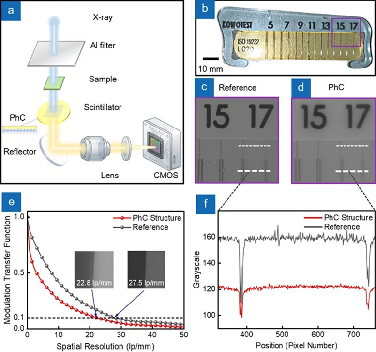
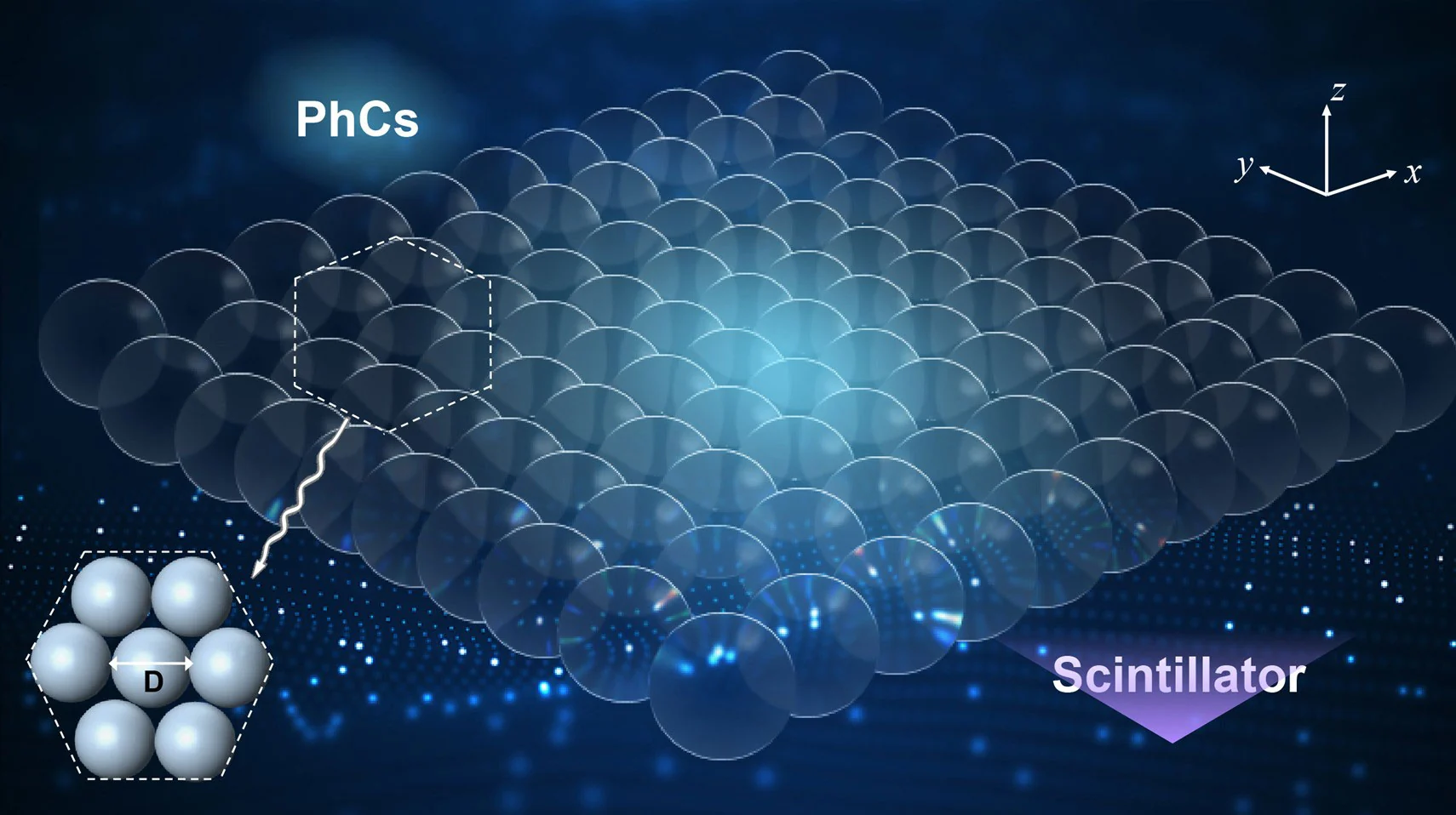
Rather than increasing the thickness of the material, the research team tried to change the way light escapes from inside the scintillator. They built a layer of photonic crystal structure on the surface of GAGG:Ce crystal, which helps release the light originally trapped inside the material through periodic arrangement at the nanoscale.
Photonic crystal is a material with a regular periodic microstructure that can change the way light propagates in it. The researchers used the Bragg diffraction effect to provide additional momentum to the trapped light, allowing it to break through the original propagation limitations and enter free space, where it was eventually received by an external detector. Since this method improves light extraction efficiency rather than obtaining more signals by increasing the thickness of the crystal, it can avoid some of the contradictions between signal enhancement and image clarity in traditional solutions.
However, how to fabricate such nanostructures on a large area is also a challenge in itself. Although traditional photolithography technology can precisely control structures, it requires expensive equipment and complex processes, and it is not easy to process the surface of brittle scintillation crystals. Although simple self-assembly methods are suitable for covering large areas, they are prone to problems such as missing particles, irregular arrangements, and structural cracks, which may ultimately produce image artifacts.
To solve this problem, the researchers used a self-assembly process driven by surface tension, using the so-called Marangoni effect to control liquid flow.
The research team used a combination of ethanol and water to create a flow through the difference in surface tension between the two liquids, thereby guiding the polystyrene nanospheres to align themselves. Subsequently, the researchers used surfactants to increase the density of the particle arrangement, and transferred the assembled structure to a 25 mm diameter GAGG scintillation crystal wafer through a drainage process that avoids vibration interference.
The final photonic crystal is composed of a continuous layer of polystyrene nanospheres, with the particles arranged in a hexagonal close-packed arrangement. This structure can effectively improve the light extraction efficiency of the crystal surface.
The research was led by Associate Professor Peng Feng of Chongqing University, and the collaborative team also included Dr. Ding Yuchong of the 26th Research Institute of China Electronics Technology Group Corporation, and Liu Kaifeng, a doctoral student at Stevens Institute of Technology. Relevant papers have been published in the journal Opto-Electronic Advances.
This technology may be used in many fields in the future. In terms of medical imaging, if the detector can obtain a strong enough signal at a lower X-ray exposure, there is an opportunity to reduce the radiation dose received by the patient while maintaining image quality. For security inspection equipment, it may help the system identify more subtle object features; in the field of industrial non-destructive testing, it is also expected to improve the ability to detect internal defects and tiny structures in materials.
What is particularly noteworthy is that this technology targets imaging problems under low photon number conditions. In an environment with limited radiation dose or weak X-ray signal, it is often difficult for detectors to distinguish the real target signal from background noise. The significant improvement in light collection efficiency is expected to improve this situation.
Of course, this technology is still some distance away from large-scale commercial applications. The researchers pointed out that residual defects in the nanostructure may still affect the spatial resolution. It is necessary to further optimize the self-assembly process and verify whether this method can be applied to other types of scintillation materials.
If these problems can be solved, the new photonic crystal scintillator may provide a new design idea for the next generation of X-ray detectors: instead of simply relying on increasing the thickness of the material to enhance the signal, the new photonic crystal scintillator may release the light that has been generated more effectively while improving the imaging quality.
Comments