
Abstract:
Chinese flash memory chip manufacturer Yangtze Memory Technology Co., Ltd. (YMTC) is expanding its technology layout from NAND flash memory to DRAM memory. According to information recently disclosed by Counterpoint Research, Yangtze Memory is developing low-power memory products with a data transmission rate of 9600 MT/s and plans to promote mass production at its third wafer fab in Wuhan. This means that Yangtze Memory is trying to enter the DRAM market that has long been dominated by Samsung, SK Hynix, Micron and other companies.
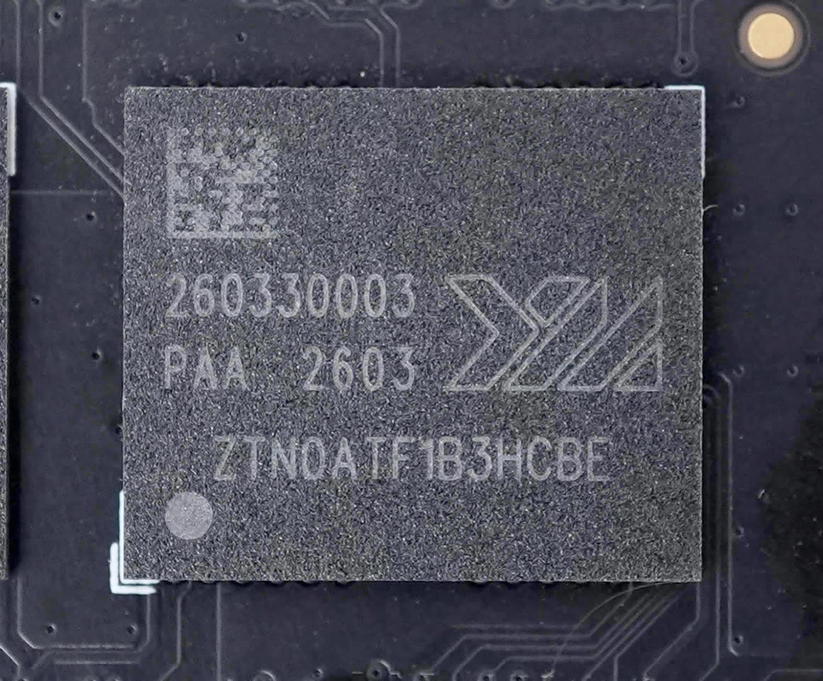
According to a report by Counterpoint Research, Yangtze Memory has been developing and testing second-generation 16Gb LPDDR5 memory at its second wafer fab since October 2025. The target data transmission rate is 7500 MT/s, and the monthly production capacity of the relevant production lines is approximately 5000 wafers. However, this project is still in the research and development and testing stages, and the report does not indicate that the product has entered large-scale commercial production.
On this basis, Yangtze Storage is also developing a higher-speed 9600 MT/s version. Different from the previous generation R&D project, the new solution plans to use vertical channel transistors (VCT) and 4F² memory cell architecture, and plans to promote mass production in the third wafer fab. It should be noted that the existing information describes R&D goals and future production plans, and does not confirm that the 9600 MT/s product has completed verification or officially entered mass production.
The key to this technical route is how to further reduce the area occupied by DRAM storage cells. Traditional DRAM usually adopts 6F² memory cell layout, where F represents the minimum feature size in process design. The 4F² architecture attempts to reduce the plane area occupied by each memory unit by vertically arranging transistors and other structures, thereby increasing the storage capacity that can be integrated per unit chip area.
If the 4F² architecture can achieve stable manufacturing under advanced processes, there will theoretically be an opportunity to increase the integration density of DRAM chips and create room for reducing unit capacity costs. However, this architecture also faces challenges in transistor structure, manufacturing process, leakage control, reliability and yield. Even if a laboratory prototype can reach the target speed, it does not mean that it has the comprehensive performance required for large-scale commercial production.
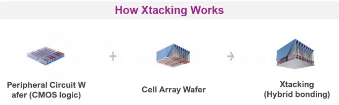
Yangtze Storage’s choice of this direction is related to its existing technology accumulation. The company is famous for its NAND flash memory business. Its Xtacking technology improves the flexibility of flash memory design and manufacturing by manufacturing the storage array and peripheral circuits separately and then integrating them through bonding. Counterpoint Research believes that Yangtze Memory is trying to extend relevant technical experience to the DRAM field. However, there are obvious differences in the storage unit structure, working mechanism and manufacturing requirements between NAND and DRAM. It cannot be simply believed that success in the flash memory field can be directly copied to the memory market.
It is worth noting that Yangtze Storage is not the only Chinese storage manufacturer trying the 4F² architecture. Another DRAM manufacturer, Changxin Memory (CXMT), is also exploring this technology route and plans to launch DDR5 registered dual in-line memory modules based on the 4F² architecture by the end of 2026. However, the plan also faces uncertainties in technical verification and mass production feasibility.
International storage giants are cautious about the prospects of the 4F² architecture. Micron Technology has previously publicly questioned the fundamental problems in the further shrinkage of this memory unit structure, believing that there are still insurmountable technical obstacles to its large-scale application. This reflects that the current DRAM industry has not yet reached a unanimous judgment on the technical route of the next-generation memory cell architecture. Whether Yangtze Storage and Changxin Storage can solve these problems through different engineering designs remains to be verified by subsequent products and manufacturing data.
At the same time, the timing of Yangtze Memory's entry into the DRAM market is also related to changes in supply and demand in the global storage industry. The rapid expansion of artificial intelligence data centers has driven the growth in demand for high-bandwidth memory, server DRAM and solid-state drives. Samsung, SK Hynix and Micron are investing a lot of resources into artificial intelligence-related storage products, and the memory used in ordinary computers and smartphones is also affected by changes in the supply structure. For Chinese manufacturers, if they can steadily launch DRAM products with qualified performance and competitive cost, they will have the opportunity to increase the market share of domestic memory.
However, the impact of this research and development plan on the global memory market cannot be overestimated in the short term. Counterpoint Research pointed out that the research and development progress of Yangtze Memory's 9600 MT/s products, customer verification status, and the mass production execution status of the third wafer fab are all indicators that need to be closely observed in the future. There is currently insufficient public information to prove that the product has achieved target performance, and there is no clear mass production schedule, production data or manufacturing yield information.
In addition, 9600 MT/s is only one of the data transfer rate indicators and cannot alone determine the overall competitiveness of memory products. For low-power memories such as LPDDR5X, power consumption, heat dissipation, stability, capacity, packaging scheme, compatibility and cost are equally important. Even if Yangtze Memory can eventually achieve this speed, it will still need to be verified by terminal manufacturers before it can enter the supply chain of smartphones, laptops or other devices.
From a longer-term perspective, Yangtze Storage is trying to break the original business division of labor in China's storage industry. In the past, Yangtze Memory's core business was NAND flash memory, while Changxin Memory mainly developed DRAM memory. Today, both companies are exploring each other's markets, and future competition may not only involve product speed and price, but also extend to manufacturing processes, memory cell architecture, patent layout, and production capacity scale.
In general, Yangtze Memory has developed 9600 MT/s LPDDR memory and plans to promote mass production in its third wafer fab, showing that it is actively expanding its DRAM business. But this is still a plan that needs to undergo technical verification and large-scale manufacturing testing, rather than a mature product that is already on the market. In the future, what will really determine whether it can challenge the international storage giants will be product performance, manufacturing yield, cost control and the ability to continue to expand production capacity.
Comments