
Abstract:
The bare die photos of Intel’s next-generation Nova Lake mobile processor were recently released by the YouTube channel Moore’s Law Is Dead. Based on this, the chip layout and core configuration of the two solutions, Nova Lake-HX and Nova Lake-H, can be sorted out. However, the relevant photos and parameters are all from unofficial leaks. Intel has not yet confirmed the model, specifications or manufacturing process, and the specific information may still be adjusted.
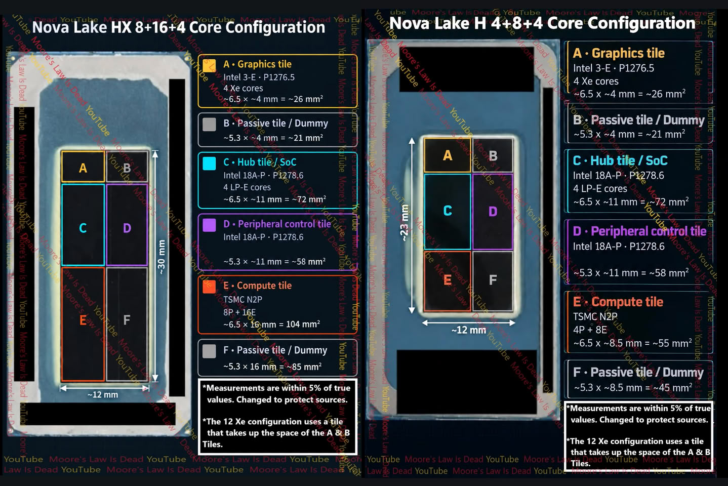
It was revealed that the higher-positioned Nova Lake-HX uses 8 performance cores, 16 energy-efficiency cores and 4 low-power energy-efficiency cores, for a total of 28 cores. The chip package is said to be composed of six functional or structural core particles, with an overall size of approximately 12×30 mm and an area of approximately 360 square millimeters. The layout listed in the report includes a graphics core of approximately 26 square millimeters that integrates four Xe graphics cores; a core of approximately 72 square millimeters that carries 4 low-power energy-efficiency cores and serves as a central hub; a peripheral control core of approximately 58 square millimeters; and a computing core of approximately 104 square millimeters that carries 8 performance cores and 16 energy-efficiency cores. Two other pieces are described as passive cores for structural support, with areas of approximately 21 and 85 square millimeters respectively. The above areas are all estimates from the news.
The lower-end Nova Lake-H is said to use 4 performance cores, 8 energy-efficiency cores and 4 low-power energy-efficiency cores, for a total of 16 cores; the package size is approximately 12×23 mm and the area is approximately 276 square millimeters. Its graphics, central hub and peripheral control core are said to be the same as the HX version. The main change is that the computing core is reduced to about 55 square millimeters, and a passive core of about 45 square millimeters is provided. According to reports, the computing cores of these two processors may be manufactured by TSMC's N2P process. Some hub and control cores use Intel 18A-P, and the graphics cores use Intel 3-E. The division of labor between these processes and cores has not yet been confirmed by Intel.
If the news is true, Nova Lake-HX will continue the route of high-performance gaming notebook processors favoring desktop-level chip packaging, while Nova Lake-H will serve mainstream high-performance notebooks with fewer CPU cores. Multi-chip design allows different functional modules to use different processes, but actual performance, power consumption, heat dissipation, yield and cost still depend on the chip interconnect and the entire platform design. Previous news that Nova Lake-HX may adopt the Core Ultra 4000 name and product release time also came from leaked information.
Currently, Intel has not announced the official product specifications of Nova Lake-HX and Nova Lake-H, nor has it confirmed the number of cores, number of Xe graphics cores, package size, die process or time to market. Key parameters such as clock frequency, power consumption, cache capacity, memory support and actual performance are still unknown. At this stage, these photos and configurations should be regarded as early leaks rather than final product specifications.
Comments