
Abstract:
As high-bandwidth memory (HBM) technology evolves to higher-layer stacks, heat dissipation and yield issues are becoming new challenges facing the industry chain. The latest news shows that Samsung Electronics and SK Hynix plan to significantly increase the supply of 8-layer HBM4 memory for Nvidia's next-generation AI accelerator Rubin Ultra starting from the second quarter of 2027, instead of the previously widely optimistic 12-layer stacking solution.
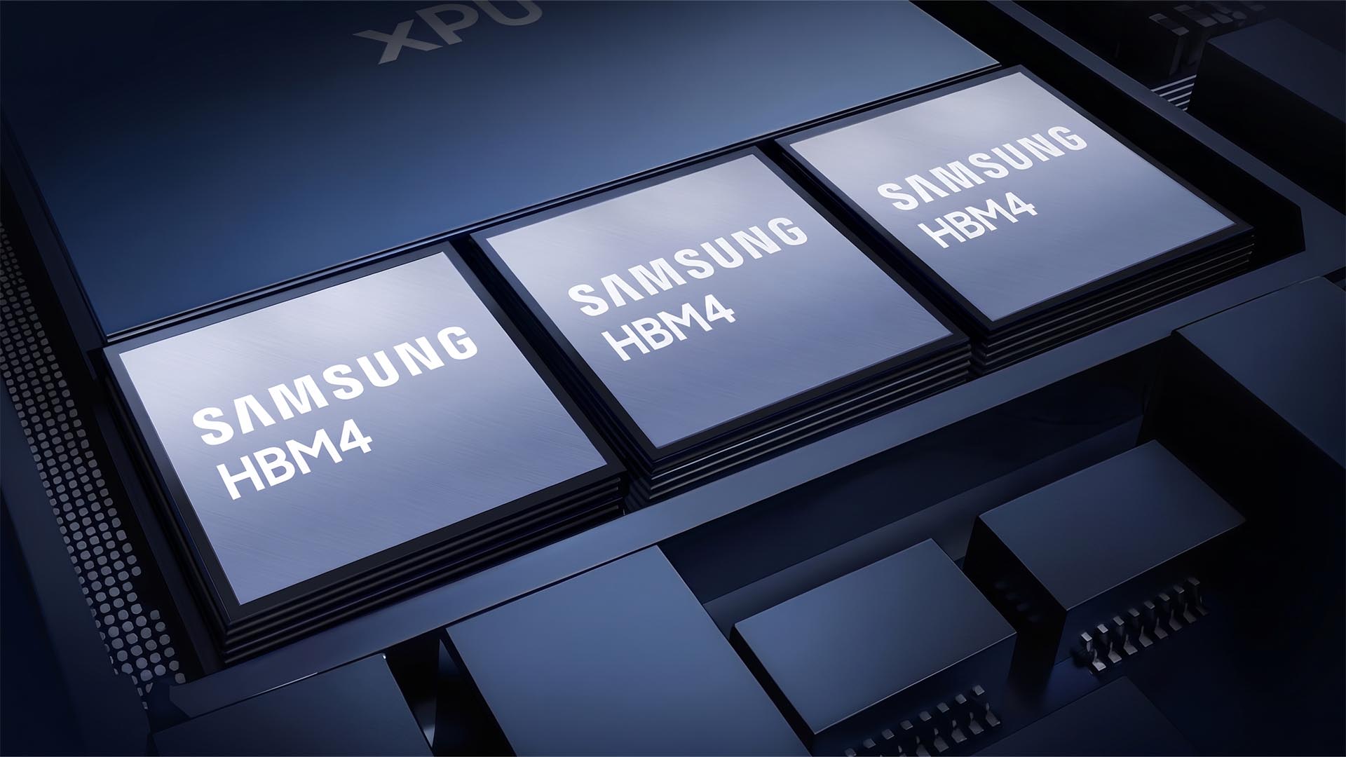
It is reported that Nvidia has started discussions with Samsung and SK Hynix in the third quarter of 2026, hoping to introduce more 8-layer HBM4 configurations for future products. Although the market had previously believed that the Rubin series would mainly use more advanced 12-layer HBM4 or HBM4E memory, supply chain realities prompted the company to re-evaluate this plan.
Industry analysts believe that the core of the problem is not performance, but manufacturing difficulty. As the number of DRAM chip layers continues to increase, each additional layer will increase the thermal resistance, making heat dissipation more difficult. It also increases the probability of defects in wafer bonding, resulting in a decrease in overall yield. In contrast, although the 8-layer stack compromises on single stack capacity, it is easier to manufacture and cool, so it is regarded as a compromise that takes into account cost, productivity and stability.
However, this does not mean that 12-layer HBM4 will be abandoned. Currently, Samsung and SK Hynix are still mass-producing 12-layer HBM4 products and have obtained NVIDIA certification. In the next few years, 12-layer HBM4 is expected to remain an important part of the high-end HBM market, but starting from mid-2027, the market share of the 8-layer version is expected to increase significantly.
According to information disclosed by Korean media, Samsung and SK Hynix also need to obtain independent certification for 8-layer HBM4. The two companies are currently preparing relevant parts, materials and quality verification processes. Since the technical complexity of the 8-layer solution is lower than that of the 12-layer solution, industry insiders believe that subsequent certification is relatively difficult and there is unlikely to be another major delay.
It is worth noting that NVIDIA is not only evaluating 8-layer HBM4, but also studying the 8-layer HBM4E solution. The final configuration will depend on the design needs, supply capabilities and overall cost structure of Rubin Ultra and its NVL cabinet-level system.
At the same time, the Rubin Ultra project itself has also seen some adjustments. It was previously expected that the product would use a more radical large-scale chip design, but supply chain pressure has prompted Nvidia to scale back some plans. According to reports, Rubin Ultra has been adjusted from the original more complex solution to a dual-chip design to reduce manufacturing risks and ensure mass production progress.
As a new generation of AI computing platform that NVIDIA plans to launch in 2027, Rubin and Rubin Ultra will succeed the Blackwell series and become the company's flagship products. The current partial pullback of HBM4 from 12 layers to 8 layers also reflects that the AI industry is shifting from purely pursuing parameters and stacking height to a realistic stage that pays more attention to yield, heat dissipation and supply stability.
Comments