Scientists have invented a ground-breaking microscope capable of capturing the reaction of surfaces to light with a remarkable resolution of just 1 nanometer. This advance makes it possible to observe structures at the atomic scale, including individual molecules and tiny defects. Being able to observe these features is an important step forward for developing and improving nanomaterials and surfaces at extremely small sizes (on the angstrom scale).
Scattering near-field optical microscopy with ultralow tip oscillation amplitudes. Image source: Takashi Kumagai
Studying how light interacts with matter at such tiny scales is crucial to advances in technology and materials science. Atomic-level features, such as defects in diamonds or individual molecules in electronic devices, can have a significant impact on the behavior and performance of materials. To truly understand and manipulate these effects, optical microscopy must continue to evolve to reach these smaller scales.
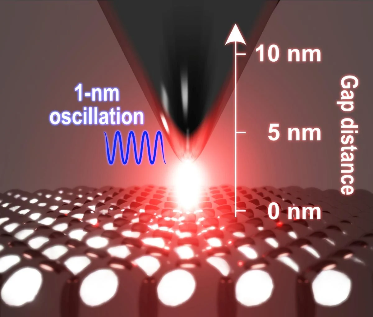
Researchers at the Fritz-Haber Institute of the Max Planck Society in Germany and their international collaborators from the Institute of Molecular Science/University of Comprehensive Research (SOKENDAI) in Japan and CIC nanoGUNE in Spain have developed a scattering-type scanning near-field optical microscopy (s-SNOM) method with a spatial resolution of 1 nanometer. The technology, called ultra-low tip amplitude s-SNOM (ULA-SNOM), combines advanced microscopy methods to visualize materials at the atomic level.
Traditional s-SNOM methods use a laser-irradiated probe tip to scan the surface, typically achieving resolutions of 10 to 100 nanometers. However, this is not enough for atomic-scale imaging. By combining s-SNOM with non-contact atomic force microscopy (nc-AFM) and using a silver probe tip under visible laser illumination, the researchers created a plasmonic cavity (a special light field) that was confined to a tiny volume. This allows for fine optical contrast on the angstrom scale.
This approach allows scientists to study materials at the smallest scales and could potentially lead to advances in the design of new materials for electronics or medical devices. Being able to image features such as atomic defects and nanoscale structures with such high precision opens up new possibilities in optical engineering and materials science.
Altogether, this development provides a valuable tool for characterizing surfaces with atomic-level precision, contributing to future advances in single-molecule and atomic-scale optical microscopy.
Compiled from /scitechdaily