
Abstract:
The technical indicator forecast of the domestic DRAM manufacturer Changxin Technology’s next-generation memory technology platform G6 has recently leaked.
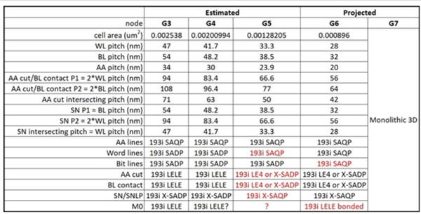
The plan shows that Changxin will continue to use the DUV lithography process to produce G6-generation memory, which is expected to be launched as soon as 2028. The chip unit area will be further reduced from 0.00128205 square microns in the G5 generation to 0.000896 square microns, a reduction of 30%.
In the absence of EUV lithography machines, Changxin is approaching the physical limits of this technology through in-depth optimization of the DUV process combination.
According to forecast data released by X platform technician Frederick Chen, the unit area shrinkage of G6 will be achieved by continuing to optimize the 193nm DUV immersion lithography machine, combined with self-aligned quadruple patterning (SAQP) technology, and some levels will use the self-aligned double patterning (SADP) process.
From the perspective of process node indicators, the WL (word line) spacing of G6 will be further tightened from 33.3 nanometers of G5 to 28 nanometers, the BL (bit line) spacing will be reduced from 38.5 nanometers to 32 nanometers, and the AA (active area) spacing will be reduced from 23.9 nanometers to 20 nanometers.
The photoresist solution will be upgraded simultaneously. The AA cutting layer will be upgraded from 193i LE4 to 193i LE4 or X-SADP, and the X-SADP option will also be introduced for the bit line contact layer.
The first introduction of the bonding process is the most critical technical variable in the G6 plan.
In the forecast table, the M0 layer of G6 is marked as "193i LELE bonded", which means that Changxin plans to use wafer-level hybrid bonding to decouple the DRAM storage array from the peripheral logic circuits and then stack the interconnects.This idea is highly consistent with Changxin’s technical layout on the 4F² architecture. Cao Kanyu, President of Changxin Technology, made it clear at the 4th Integrated Chip and Chip Conference that one of the core breakthroughs of the 4F² architecture is to decouple DRAM from CMOS processes and then achieve high-speed interconnection through wafer-level hybrid bonding. This is a key turning point for DRAM from two-dimensional scaling to three-dimensional integration. Changxin expects to launch a new generation of DDR5 RDIMM products incorporating this technology by the end of this year.
G6 may be the last generation product of 6F² memory chip structure. The forecast points out that
Changxin has laid out 3D memory technology in advance, and its 3D DRAM stacking layers can reach more than 64 layers. It is expected that the G7 generation products launched after 2030 may shift to 4F² structure or 3D memory architecture.
Comments