
Abstract:
IBM and Siemens announced joint research to advance the NanoStack transistor architecture announced by IBM this year, focusing on the development of tools and processes required for next-generation chip design, simulation and manufacturing. IBM is responsible for semiconductor device technology, and Siemens will contribute capabilities in electronic design automation, process simulation, lithography optimization and advanced manufacturing software. The two parties plan to build more sophisticated virtual models to simulate performance, optimize designs and identify processing problems before actually manufacturing chips.
The core idea of NanoStack is to change the transistors that are traditionally arranged side by side into vertical stacks, and to arrange different layers in a staggered manner, so as to break through the limitation of continuing to shrink the distance between transistors on a two-dimensional plane. IBM said that the new architecture can use different combinations of materials for each layer to optimize transistor performance and power consumption respectively; by stacking N-type and P-type transistors on top of each other, designers can also choose materials and wiring methods more flexibly. IBM describes it as the industry's first known nanosheet-based three-dimensional transistor design.
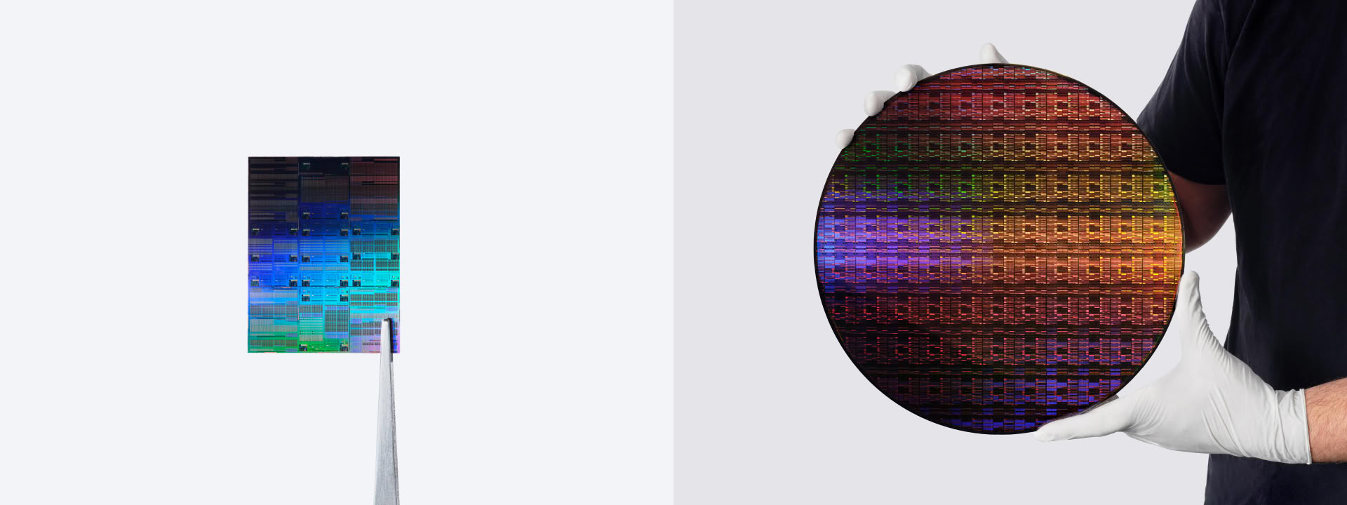
In June this year, IBM announced the results of its 7-nanometer (0.7 nanometer) technology research, saying that nearly 100 billion transistors can be integrated on a chip the size of a fingernail, with a density approximately twice that of its 2-nanometer chip. The "0.7 nanometer" refers to the technology node name, not the actual size of each transistor in the chip. The paper results released by IBM estimate that compared with its 2-nanometer node, the new technology can bring about a maximum performance improvement of about 50%, or reduce energy consumption by about 70% when the performance is equivalent; other studies show that the NanoStack architecture can reduce the SRAM area by about 40%. These figures belong to IBM's calculations and predictions of research technology, and are not the actual measured performance of mass-produced products.
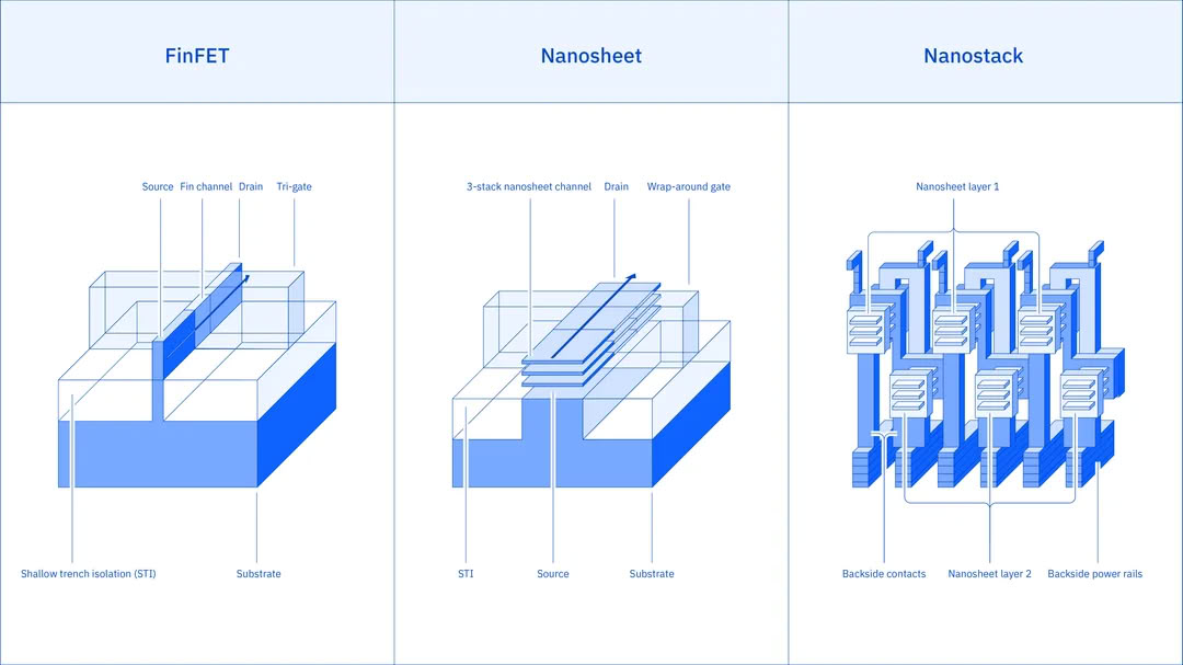
IBM previously stated that the research team has verified the feasibility of actual manufacturing and computing of the NanoStack structure through experiments such as ultra-thin dielectric bonding, dual-channel engineering, and normally switching CMOS inverters. However, moving from laboratory samples to mass production still requires solving problems such as wafer bonding and alignment, interlayer heat dissipation, micro-wiring, backside power supply, and three-dimensional inspection. IBM has said that it may advance to the production stage as early as the next five years, but this cooperation announcement with Siemens did not announce a specific development timetable, investment amount or commercial mass production customers.
The focus of this cooperation is to establish a tool chain that allows complex three-dimensional transistors to be designed, simulated, and manufactured, rather than announcing that new chips have been put into production. IBM and Siemens hope to collaboratively optimize device physics, chip design software and manufacturing processes to lay the foundation for subsequent generations of NanoStack and technology research and development beyond the 7-nanometer node.
Comments